Featured video
Advanced packaging
More microelectronics stories

Fueled by creativity: Graduate student completes six-year ASU journey without pause
From the moment she began her undergraduate studies, Olivia Reyes was determined to immerse herself in the intersection of art and technology. In just six years — without taking a break between her bachelor's degree and master’s degree — she completed both at Arizona State University’s School of Arts, Media and Engineering.

First-ever Taiwan Symposium at Thunderbird celebrates business, cultural connections
The investment by TSMC and other Taiwanese corporations in Arizona will reap dividends not only in thousands of new jobs but also in strengthened cultural connections and new methods of sustainability. That was the message embraced at the first-ever Taiwan Symposium sponsored by ASU’s Office of Global Academic Initiatives and hosted at the Thunderbird School of Global Management.

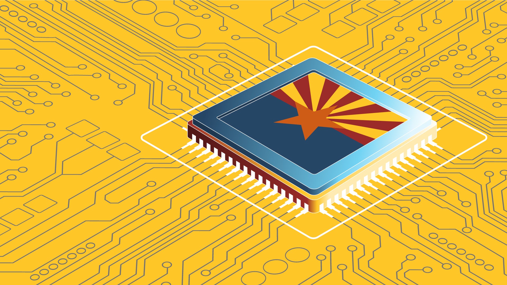
ASU at the heart of the state's revitalized microelectronics industry
A stronger local economy, more reliable technology, and a future where our computers and devices do the impossible: that’s the transformation ASU is driving through its microelectronics research right here in Arizona.

ASU in position to accelerate collaboration between space, semiconductor industries
Leaders across the space industry converged in Tempe March 19–20 for the third annual Arizona Space Summit, a statewide effort designed to elevate Arizona as a premier hub for the space sector.

Building bridges in India
Fulton Schools Dean Kyle Squires visited India to explore research and education collaboration with Indian government, higher education and industry leaders.

Extended reality class prepares students for semiconductor industry
Fulton Schools Associate Professor Umberto Celano is using extended reality technology in the classroom to enhance semiconductor metrology methods for students.