image title

5 who work for social justice honored with MLK awards at ASU

ASU honors 5 who work to continue Martin Luther King's legacy.
January 20, 2022

Founding director of Project Humanities is first Faculty Servant-Leadership Award winner

The legacy of Martin Luther King Jr. reminds us to cultivate integrity in our lives along with happiness, according to Neal Lester, the founding director of Project Humanities at Arizona State University.

“I’m continually trying to respond to his call for maintaining integrity and truth that he framed as justice, peace and the social transformation and reclamation of our individual and shared humanity,” said Lester, a Foundation Professor of English at ASU.

He spoke at the 37th annual ASU Dr. Martin Luther King Jr. Celebration at Sun Devil Stadium on Thursday, where he was honored as the inaugural Faculty Servant-Leadership Award winner.

“For me, this annual holiday and recognition from my ASU community is but another opportunity to be better and to do better,” he said. “For me, doing and being better is being mindful of living and practicing those values that Project Humanities calls Humanity 101, those simple values of respect and integrity and compassion and forgiveness and empathy and kindness and self-reflection.”

Lester was among five people honored as 2022 ASU Dr. Martin Luther King Jr. Servant-Leadership Award winners. The other four were:

• Marcelino Quiñonez, an ASU alum, playwright, former high school teacher and the current director of educational outreach and partnerships at ASU.

• Roicia Banks, an ASU alum, current student and founder of Social Roots LLC, a social work practice for Black and Indigenous families.

• Ivan Quintana, an ASU student who works as a student support specialist at Mesa Community College, which he attended before transferring.

• Silvana Salcido Esparza, chef and owner of Barrio Café in Phoenix and a community activist.

The breakfast celebration was just one of several events sponsored by the MLK Committee at ASU, according to Colleen Jennings-Roggensack, vice president of cultural affairs at ASU who served as the emcee of the event. The celebration included the winners of the statewide poster and essay contests for K–12 students, several of whom read their essays.

This is the first time that the 2022 Student Servant-Leadership Award was given to two students in one year, Jennings-Roggensack said. Banks and Quintana, both first-generation college-goers, were awarded $2,000 scholarships.

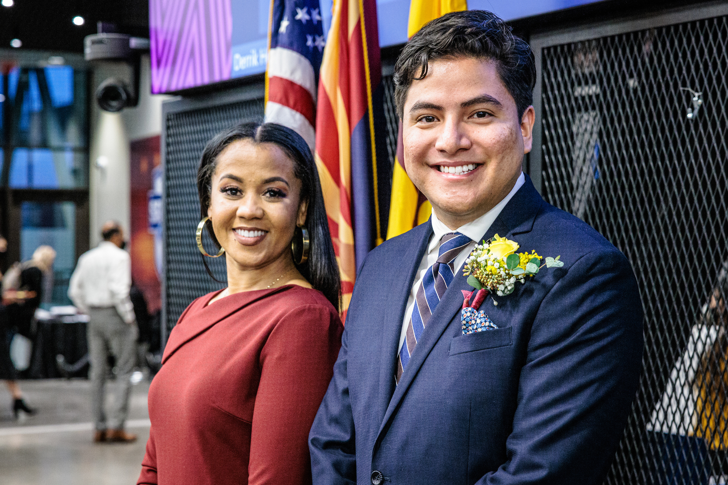
Roicia Banks and Ivan Quintana were the winners of the ASU MLK Student Servant-Leadership Award. This was the first time two students were chosen. They won $2,000 scholarships. Photo by Charlie Leight/ASU News

Banks graduated with bachelor's degrees in political science and African and African American studies at ASU. She then received a master’s degree in social work from the University of Houston. She is currently working toward a Master of Legal Studies degree with an emphasis in Indigenous law at the Sandra Day O’Connor College of Law at ASU.

She is a Black and Indigenous woman who was in foster care as a child before being adopted into a Hopi family. Her mother died of COVID-19 last year.

“It’s been a trying year personally and professionally,” she said at the breakfast celebration.

Banks worked as a social worker for state and tribal governments before starting Social Roots LLC.

“Thank you to my community,” she said. “I would not be able to do the work I do if nobody in my community saw the value in it.”

Quintana moved from a small town in northern Mexico to the U.S. at age 18 to attend Mesa Community College, where he took classes in addition to working full time.

His experience navigating the higher education system led him to became a college completion ambassador for the AmeriCorps Arizona Ready for College and Career program, helping high school seniors apply to college and complete the FAFSA form. 

He transferred to ASU in 2019, where he is a senior double majoring in criminal justice and criminology and public service and public policy. He plans to attend law school. 

Quintana told the crowd that he was reflecting on the theme of this year’s breakfast celebration: “Inclusion starts with us.”

“The truth is that inclusion and empathy of Dr. King sets a higher standard, where we have to challenge ourselves to include people that not only don’t look like us but might be against us,” he said. 

He recalled how King met with segregationists.

“Love and empathy is what binds all of us, and all humanity is worthy of dignity and redemption.”

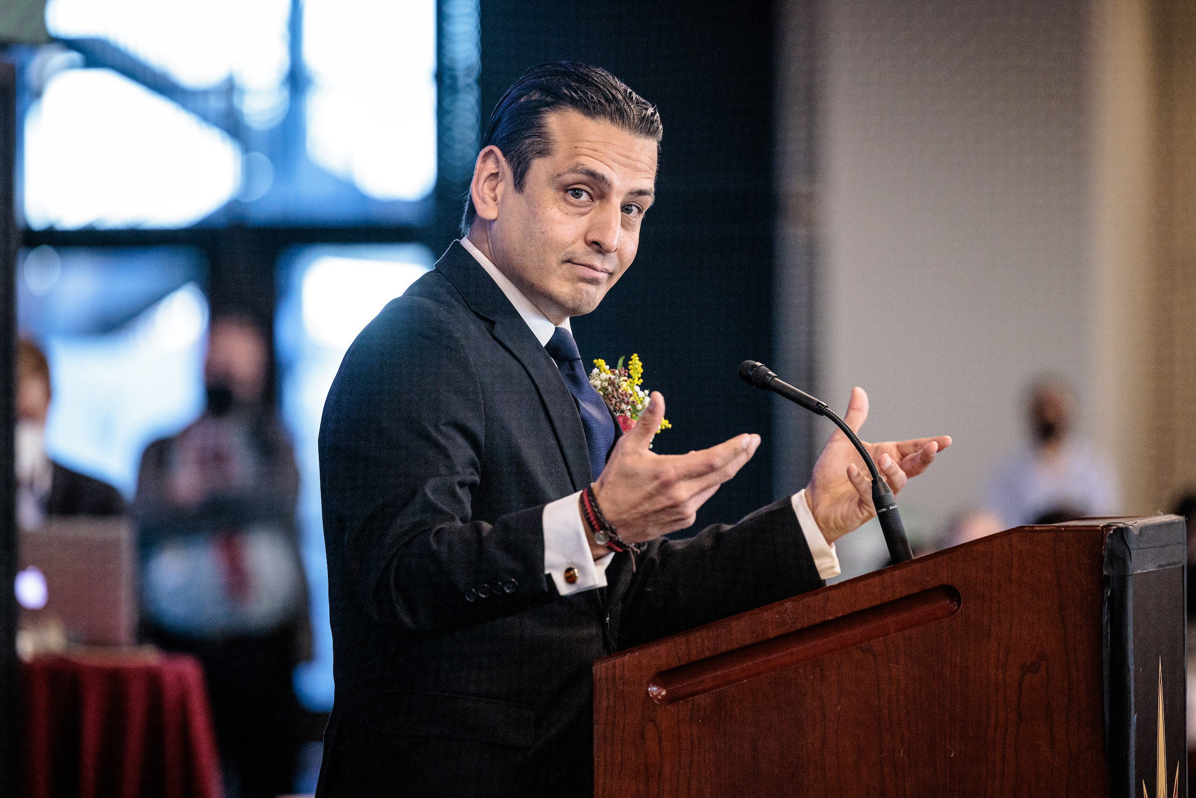
Marcelino Quiñonez, an ASU alum and the current director of educational outreach and partnerships at ASU was the winner of the inaugural ASU MLK Staff Servant-Leadership Award for 2022. Photo by Charlie Leight/ASU News

 This year, the committee also gave out the first-ever Staff Servant-Leadership Award, to Quiñonez, who in December was appointed to represent District 27 in the Arizona Legislature.

He shared his favorite King quote: “The arc of the moral universe is long, but it bends toward justice.”

“I believe it bends toward justice because of what we can all do every single day to lend a hand, to make sure everyone eligible to vote has the right to vote,” he said. 

Jennings-Roggensack became emotional as she introduced Esparza, whom she has known for years, as the 2022 Community Servant-Leadership Award winner.

“She cooked meals for health care workers and those in need” during the pandemic, Jennings-Roggensack said.

“And she gave up her health insurance to feed other people.”

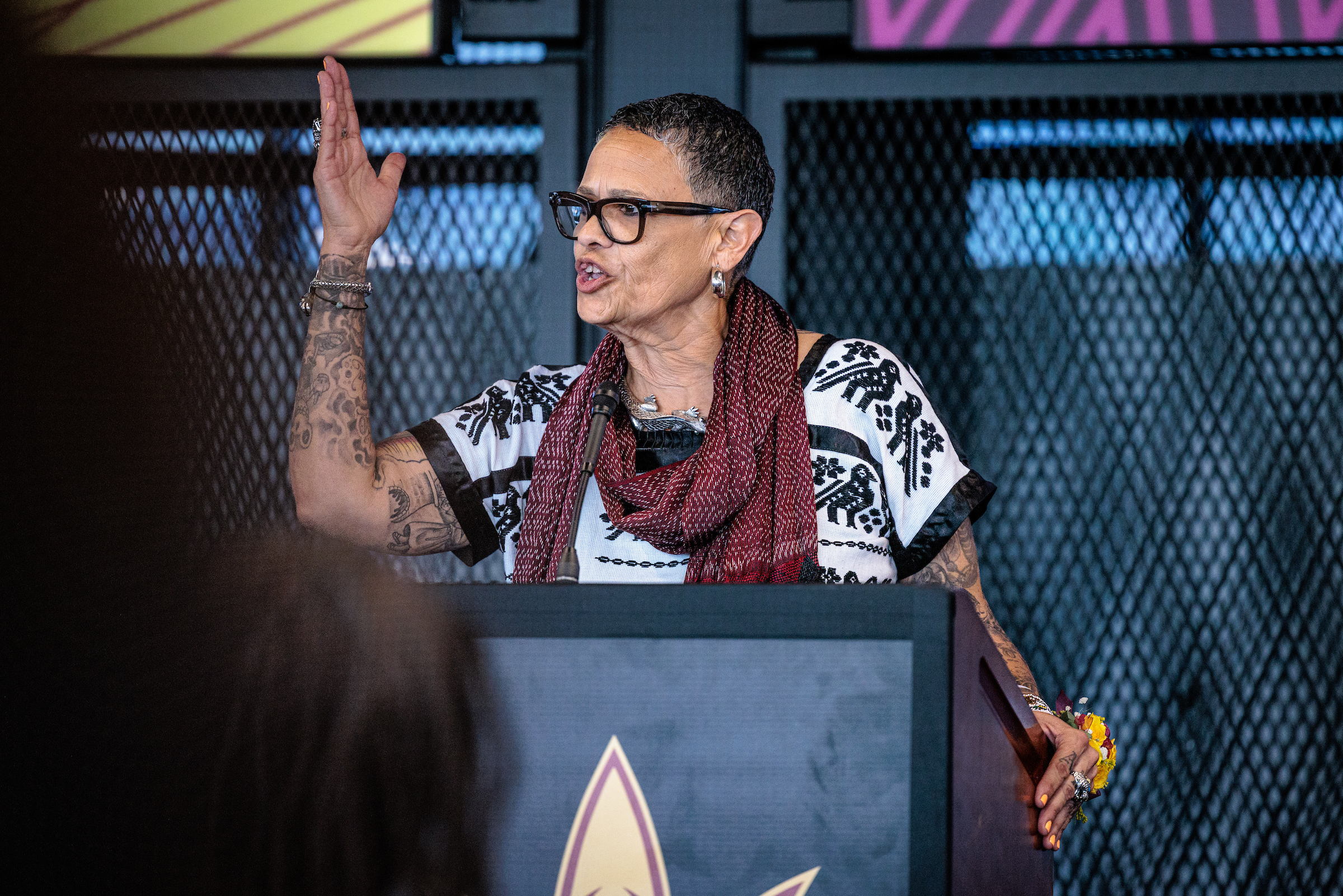
Silvana Salcido Esparza, chef and owner of Barrio Cafe, won the ASU MLK Community Servant-Leadership Award for 2022 for her community activism during the pandemic. Photo by Charlie Leight/ASU News

Esparza told the crowd how she used to accompany her father when he preached at migrant camps in central California. She would smell the tortillas the impoverished workers made, but rarely meat.

“That influenced me,” she said.

“Where are we today? Instead of going forward, we’re going backward.”

She said that politicians and educators must act to help poor people.

 “You cannot fight hate — and there’s a lot of it out there — with hate. You gotta fight it with love.”

Top photo: Neal Lester, Foundation Professor of English and founding director of Project Humanities at ASU, speaks to the crowd at the 37th Annual ASU Dr. Martin Luther King Jr. Celebration at Sun Devil Stadium on Jan. 20. He was the winner of the inaugural ASU MLK Faculty Servant-Leadership Award. Photo by Charlie Leight/ASU News

Mary Beth Faller

Reporter , ASU News

480-727-4503

 
image title

ASU a major player in microelectronics

January 20, 2022

University experts share insights about this microscopic world

The field of microelectronics plays a macro-sized role in our lives. It’s responsible for the tiny brains — microchips — that power most electronic things these days: familiar technology like smartphones and TVs, important medical equipment from hearing aids to MRI scanners, and even everyday appliances like microwave ovens and thermostats.

Our dependence on microchips is now underscored by the shortage that’s stalling the production of cars and cell phones. For supply and security reasons, there’s growing interest in making more semiconductors and microchips in the U.S.

With its cutting-edge facilities, strategic partnerships, educational programming and research capability, Arizona State University is positioning Arizona as the perfect hub for this growing industry.

MORE: How ASU and industry partners are boosting the semiconductor business in Arizona.

What’s the difference between microelectronics, semiconductors and microchips?

Basically, semiconductors are used to make microchips, microchips are physical devices you can hold in the palm of your hand, and microelectronics refers to the field or industry as a whole.

Semiconductors are a type of material with the traits of both conductors, like aluminum, and insulators, like glass. Semiconductors such as silicon have enabled us to make electronic devices smaller, faster and more reliable.

They usually come to fabrication plants as a thin, flat wafer, similar to a dinner plate.

“When you have lots of different layers of semiconductors in various structures, you get devices like transistors, and devices wired together become microchips,” says Zachary Holman, an associate professor in the School of Electrical, Computer, and Energy Engineering.

Nowadays, people often use the term “semiconductors” as a shorthand for chips and other devices made with semiconductor materials.

Holman's face reflected in a silicon wafer

Zachary Holman is reflected on a silicon wafer at the ASU MacroTechnology Works building at ASU Research Park.

How small are microelectronic devices?

The “micro” stands for micrometer, which is one-millionth of a meter. (An average human hair is around 60 micrometers thick.) Microchips themselves aren’t that tiny, but if you stuck one under a microscope, it would have features and regions at that micrometer scale. Today, some chips even have features on the nanometer scale. A nanometer is one-billionth of a meter.

In 2021, the tech industry hailed the improved capacity of a supercomputing chip the size of an iPad, along with the creation of the world’s smallest single-chip system the size of a dust mite. Despite the dramatic size difference, both are microelectronic devices, because both have micrometer-scale features.

The microchips found in everyday computers and smartphones range from the size of a fingernail to a postage stamp.

How are microchips made?

The manufacturing process has become much more sophisticated since the first microchip made its debut in 1959.

It starts with design — engineers use a software program to lay out the microchip’s structure, like an architect creating the blueprint of a house.

The design goes to a fabrication plant — often called a fab for short, or sometimes a foundry — which takes a base semiconductor wafer and layers different materials like metals, oxides and other semiconductors on top of it.

“They also do patterning steps, which are similar to the old camera film exposure processes. After depositing a layer, the wafer goes into a chemical bath or a gaseous environment that removes material from select areas, while other areas are protected,” Holman says. “That process gets repeated up to hundreds of times to form all of the elements for that chip’s design.”

These patterning steps etch the layered wafer to match the initial design.

There are many chips per wafer, so once all its layers are complete, the fab “dices” it, separating out the individual chips like slices of a sheet cake. The final step is to package the chips by bonding them to circuit boards, those green plastic panels you find inside electronics. The fab ships the final creations to other manufacturers, who use them to make products such as cars, TVs and cell phones.

infographic of the microchip manufacturing process described above

Graphic by Shireen Dooling

Why is there a microchip shortage right now? Are more fabs the solution?

Manufacturers from tech, auto and other industries expected that their sales would go down during the COVID-19 pandemic, so they ordered fewer chips from fabs. However, pandemic optimism and vaccine availability in summer 2021 led to more consumer spending. Manufacturers suddenly had more demand than supply for microchip products.

Now, fabs are being flooded with additional requests as many industries try to order more chips at once.

“It's hard to increase the supply rapidly because the chip fabrication process takes months,” Holman says. “The fabs themselves are really complex and expensive. From the start of construction to a fab being operational is typically three-plus years.”

Currently, most semiconductor and chip manufacturing happens overseas, with the U.S. accounting for just over 12% of manufacturing globally, according to the Semiconductor Industry Association’s 2020 report.

Building additional fabs in the U.S. would help relieve similar global chip shortages in the future by adding to the world’s overall fabrication capability. If U.S. fabs prioritize orders from U.S. consumers, that could also help protect our domestic supply chain.

What are the national security issues to consider with microelectronics?

“Think of the U.S. Department of Defense’s computer systems, communications systems, transportation systems — they all rely on microelectronic devices to function properly,” says Nadya Bliss, executive director of ASU’s Global Security Initiative.

These devices are integral not only to military operations, but also critical sectors like health care and the economy. If any of those were compromised, Bliss says, the consequences would also impact national security.

In a recent report, the National Security Commission on Artificial Intelligence noted the need to develop a resilient microchip and semiconductor supply chain in the U.S. in order to stay ahead in the geopolitical technology arena.

“Increasing the design and fabrication of these technologies in the U.S. would address a major national security vulnerability — that an adversarial nation could tamper with the technology at some point in the supply chain,” Bliss says.

Researcher in protective gear looks over machinery

The Advanced Electronics and Photonics facility gives companies access to ASU experts and equipment so they can develop new materials, methods and designs for microelectronics at industry scale. Photo by Andy DeLisle

How is ASU helping Arizona lead the U.S. microelectronics industry?

An educated workforce is key for Arizona to become a home for microelectronics manufacturing. While ASU has been producing top-notch engineering graduates for 65 years, the Ira A. Fulton Schools of Engineering is now investing in a talent pipeline specifically for microelectronics with the creation of its new School of Manufacturing Systems and Networks.

“With the new fabrication facilities coming into the Valley from Intel and Taiwan Semiconductor Manufacturing Corp., we’re expecting over 10,000 new jobs,” says Kevin Reinhart, director of research project management at ASU’s Knowledge Enterprise.

These companies and many others can take advantage of ASU’s research expertise and specialized equipment at ASU facilities like the Advanced Electronics and Photonics facilityASU NanoFab and the Eyring Materials Center. There, they can develop new materials, methods and designs for microelectronics at industry scale.

“At ASU’s MacroTechnology Works site, we’ve got 50,000 square feet of cleanroom facilities,” Reinhart says. “From a university perspective, we’re very unique in that aspect.”

These facilities also provide opportunities for ASU students to gain the critical hands-on experience that employers want. (Find out how your company can partner with ASU.)

In addition, ASU will use funds from Arizona’s New Economy Initiative to create five Science and Technology Centers, two of which will contribute to the state’s microelectronics industry — the Energy Materials and Devices Center and the Advanced Manufacturing Center.

The university aims to bring even more funding for microelectronics to Arizona. ASU played a lead role in adding support for a domestic microelectronics industry — called the CHIPS for America Act — to the 2021 National Defense Authorization Act. If funding legislation passes, ASU will propose a National Network for Microelectronics with a university-supported core facility in Arizona.

Fabrication plants use tons of water, so why are we building them in the desert?

Water is a crucial part of the chip manufacturing process. Between adding each delicate layer of the wafer, the fab must wash away all residue so that no bacteria or particles obstruct the chips’ microscopic pathways.

But to rinse off every speck of debris, the water itself has to be extra clean — no minerals, no organic material. Fabs create what’s called ultra-pure water for this purpose, and it’s so clean that it’s actually not safe for humans to drink.

Creating ultra-pure water and washing wafers produces lots of leftover wastewater. So why bring more fabs to Arizona’s water-scarce desert?

“The important question is not, 'Do we have enough water?' but, 'How do we invest our limited water?'” says Dave White, director of the Global Institute of Sustainability and Innovation and professor in the School of Community Resources and Development. “We need to look for the most efficient water uses that have the greatest social, economic, environmental returns. I would call semiconductor manufacturing in our region a water-smart industry.”

Manufacturing brings many benefits to the state, including skilled, high-wage jobs and a supply of high-demand products. But the state benefits the fabrication plants as well — Arizona has a highly educated workforce and a low risk of environmental hazards such as earthquakes or hurricanes.

Fabs in Arizona need to be innovative and efficient with their water use and reuse, but that’s just as true for cotton fields and homes, White says.

Intel’s partnership with the city of Chandler is a prime example of how fabs can accomplish this. There, they take wastewater from Intel’s fabs and pump it back into the ground. As it filters through the earth, the water purifies naturally, and it also recharges the aquifer. Groundwater levels are concerningly low throughout the state, so the Intel-Chandler partnership is a solution for two pressing issues at once.

Researcher in protective gear transfers square piece of material between machines

Graduate student David Quispe works in the MacroTechnology Works building at ASU Research Park.

What’s next for microelectronics?

Talk about the future of microchips, and you’re sure to run into Moore’s law. It’s more of an idea than a proven scientific theory. Essentially, it says that microchips’ computational power doubles (and their size halves) about every two years. It implies that microchips will hit a limit where they can’t be improved on anymore.

Holman compares Moore’s law to a scene from “Spinal Tap” where a rock musician shows off his amplifier that goes up to 11, instead of the usual 10.

“Moore's law has been about one knob of optimization, namely making things smaller in two dimensions, and that knob has already been turned up to 11. That's why, going forward, the technical innovation in microelectronics is about building in three dimensions,” he says.

Putting different capabilities that normally exist on separate chips — such as sound, display, computation and memory — together to create an all-in-one chip is another new direction for microelectronic technology, he adds.

Additionally, microelectronics will be crucial in the shift to renewable energy. According to the U.S. Energy Information Administration, only 12.6% of our national energy consumption came from renewable sources in 2020.

“How do we get closer to a hundred percent? Well, you need to have a lot more control over where electricity is being generated, where it's being consumed and stored, and when,” Holman says.

Electronics that can share information and distribute power across the grid will allow us to draw from many renewable sources and know how much is available from a source at any given time.

With around 300 days of solar-charging sunshine every year, coupled with its microelectronics research, development and fabrication capabilities, Arizona is an ideal place to find the technological solutions we need for a future that is both sustainable and leading-edge.

Mikala Kass

Communications Specialist , ASU Knowledge Enterprise

480-727-5616