New tandem solar cell research enables greater returns from current energy infrastructure

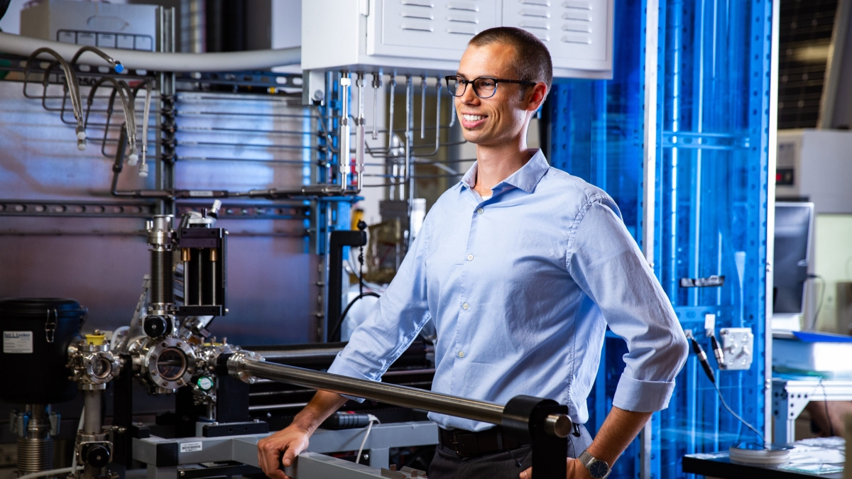
Zachary Holman and his team have published new research that can significantly increase solar cell efficiency and lower energy costs. Photo by Deanna Dent/ASU Now
Small changes can make a big difference. Powerful examples of this aphorism are new findings from the Holman Research Group within the Ira A. Fulton Schools of Engineering at Arizona State University.
Zachary Holman, an associate professor of electrical engineering, and members of his team have discovered how a microscopic alteration to industry-standard silicon wafers permits a significant enhancement to solar cell composition. The change can boost the efficiency of solar panels and lower the cost of energy production. The team’s findings have been published across two recent articles in the science journal Joule.
Almost all commercial solar panels, or modules, contain wafers made of silicon to absorb sunlight and convert it into electricity. But the inherent efficiency limits of silicon as an absorber are underwhelming.
“If you were to buy a module right now, the solar cells are probably going to offer 21% efficiency,” Holman said. This low figure reflects the fact that silicon works well only with light from a certain portion of the electromagnetic spectrum.
There are better alternatives, such as cells made from compounds like gallium arsenide. These mixed materials deliver very high cell efficiencies, but manufacturing costs are so high that their application is limited to satellites, for example.
Even so, the idea of fabricating multijunction cells, which are those with two or more different absorbers, presents a rich opportunity. At present, the terrestrial use of these composite cells is negligible, but the new research by Holman and his team offers a viable means to quickly bring two-junction, or tandem, cells into widespread use.
The innovation revolves around perovskites, a class of compounds named after the 19th-century Russian mineralogist Lev Perovski. They share a particular crystal structure and are formed from inexpensive substances including iodine, bromine, methylammonium, cesium and lead.
Perovskites are valuable to solar energy production because they efficiently absorb light from a different portion of the spectrum than is the case for silicon. Consequently, if successfully layered onto silicon wafers, the resulting tandem solar cells can yield higher efficiencies and, therefore, lower costs per unit of energy generated.
That said, previous work with perovskites was disappointing. Early versions of these compounds rapidly deteriorated when exposed to sunlight and oxygen.
“A decade ago, they lasted only minutes,” said Arthur Onno, a postdoctoral researcher with Holman’s group and a coauthor of one of the articles in Joule. “Now researchers can produce them to last for thousands of hours without degradation. It’s getting better and better.”
Two aspects of the new research by Holman and his team offer a promising route forward. One is altering the surface architecture of industry-standard silicon wafers to permit the creation of physically functional perovskite-silicon tandem cells. The other advance involves collecting light from both sides, or faces, of solar cells. This facilitates some chemical tweaking of the perovskites that, in turn, allows for an electrically more efficient tandem cell.
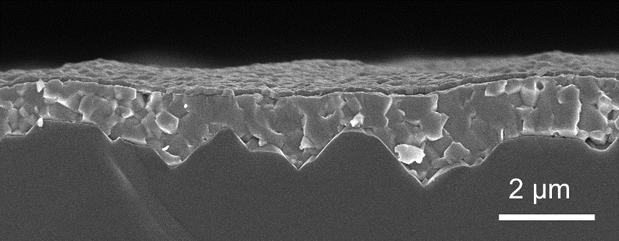
Today, commercial silicon wafers are finished with a rough texture. A magnified view would show that texture as little pyramids on the surface. These raised structures scatter the light that strikes the surface of the wafer and send it down for absorption and conversion into electricity. By contrast, a perfectly smooth silicon surface would reflect more light away and lose its benefit for energy production.
The problem for tandem cell fabrication is that those mini pyramids on the wafer surface are not small enough. A commercial silicon wafer is typically 150 micrometers thick, similar to a sheet of printer paper. Those textured pyramids on the wafer surface are only 3 to 10 micrometers high, but the layer of perovskite material applied to the top of the silicon is no more than a single micrometer.
“And when the pyramids are taller than the perovskite layer, they stick through the layer and kill the solar cell performance,” said Zhengshan (Jason) Yu, a Fulton Schools assistant research professor of electrical engineering and a coauthor of both articles in Joule. “This is why nobody tries to coat perovskite on these textured surfaces.”
The solution to this architectural problem is revealed by the new research from Holman and his group. They discovered that finishing silicon wafers to a finer surface texture, in which the pyramids are less than a micrometer tall, still scatters the light almost as effectively as standard-height pyramids. More notably, the wafers are smooth enough to allow successful application of the perovskite layer.

Layering light-absorbing perovskite material on top of silicon in a solar cell requires that the silicon texture “pyramids” are no more than a micrometer (μm) tall. Photographer: Bo Chen/University of North Carolina
Creating current compatibility
Even with this physical pairing accomplished, there remains an electrical challenge. The benefit of pairing perovskites and silicon in a tandem architecture is that they work with different parts of the electromagnetic spectrum, so the combination can collect and convert more light into electricity than either material alone.However, the different light-capturing characteristics of these two substances means that matching their current outputs is not straightforward. Since they are connected to each other in a series circuit, the lower performer will limit the current flow of the higher performer.
Specifically, the bandgap — or minimum energy threshold for light to make electrons available for conductance and energy creation — is fixed within silicon by its elemental composition. By contrast, the bandgap for perovskites is adjustable. But increasing the bandgap of perovskites to match that of silicon makes the former too physically unstable to use in any practical sense. Lowering or widening the bandgap for perovskites improves stability, but it sacrifices efficiency — and enhanced efficiency is the point of creating the tandem cell in the first place.
The Holman Research Group devised a solution by making the tandem cell bifacial. Bifaciality means using both sides of the solar cell to gather light. Bifacial cells are growing in commercial popularity, but they still represent fewer than 10% of cells in use. Moreover, bifacial tandem cells are currently nonexistent in the solar energy industry.
But the new study by the Holman group found that using the bottom of the silicon cell to collect light solved the current-matching problem.
“With our collaborators at the University of Iowa, we found that bifacial tandems can have a wide range of top-cell (perovskite) bandgaps and still have the same energy yield,” Yu said. “This synergy between tandem and bifacial technology now opens up new opportunities for ultra-high-energy-yield solar technologies.”
More immediately, the successful creation of the perovskite-silicon tandem cell by Holman’s team and collaborators at the University of North Carolina resulted in 26% efficiency — about a quarter more than current commercial single-absorber (silicon) cells.
“And while that 26% may not sound like much,” Holman said, “companies working in solar fight to secure improvements of even a fraction of a single percent.” So, this advance is notable, and Holman explains that the impact grows as you look beyond the cells or the panels.
“Making solar panels a quarter more efficient decreases the cost of solar power by significantly more than a quarter,” he said. “The panels themselves may represent only 20% of the total system cost. The balance is paying someone to configure components around your chimney, for example, and to have an electrician hook it all up. Many of these costs scale with area: bigger is more expensive. So, if you have more efficient panels, you can generate the power that you need from a smaller area, and that really brings down total system costs. It’s a leverage effect.”
These results flow from Holman’s desire to tackle practical issues in the work that he leads at ASU.
“There are countless challenges that we could work on,” Holman said. “But I want to make sure that we focus on a subset of problems where the solutions matter. In this case, we sought to determine how to adapt a material for use in an existing system, and not the other way around.”
More Science and technology

Transforming Arizona’s highways for a smoother drive
Imagine you’re driving down a smooth stretch of road. Your tires have firm traction. There are no potholes you need to swerve to…

The Sun Devil who revolutionized kitty litter
If you have a cat, there’s a good chance you’re benefiting from the work of an Arizona State University alumna. In honor of…

ASU to host 2 new 51 Pegasi b Fellows, cementing leadership in exoplanet research
Arizona State University continues its rapid rise in planetary astronomy, welcoming two new 51 Pegasi b Fellows to its exoplanet…

