Editor's note: This story is being highlighted in ASU Now's year in review. Read more top stories from 2018 here.
Dragan Grubisic knows the daunting challenge of trying to launch business startups in highly competitive tech industries.
Three-and-a-half decades of experience in various photonics and entrepreneurship endeavors have shown him how elusive the target can be on the long road from concept to commercialization.
Beyond financing, there is the research, technology development and product testing. Then there are the processing, fabrication and manufacturing operations. All that comes before marketing, merchandising and supply chain development.
Once over all those hurdles, businesses must position themselves to innovate so that new technological advances won’t eventually make their enterprises obsolete.
One example of a successful navigation of that path is the nearly 15-year-old company Grubisic leads as general manager, Laser Components DG, which has established a solid niche in the global photodetector market.
From the very beginning and over the years, Grubisic said the company — headquartered at the Arizona State University Research Park — has steadily grown and thrived in large part due to an ongoing collaboration with one of the university’s core user research facilities, NanoFab, and some of its associated faculty members.
Providing an entry point to the industry
Laser Components DG (the DG stands for Detector Group) is one of more than 100 startups and established companies that have benefitted from NanoFab’s wide array of high-tech research and development tools and the expertise of its technical staff and faculty members.
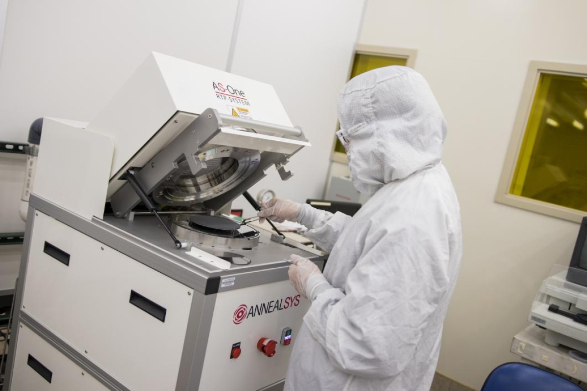
The NanoFab user facility on ASU’s Tempe campus is equipped to perform the nanotechnology engineering on which more and more of the world’s advanced electronics and photonics devices and systems are based. Its specialties are the nanoprocessing and nanofabrication required to produce prototypes of new devices from nanoscale materials.
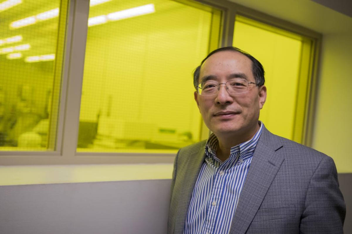
“We have the capacity for collaborations with companies that have a variety of needs,” said Yong-Hang Zhang, a professor of electrical engineering in ASU’s Ira A. Fulton Schools of Engineering. Zhang is the immediate past director of NanoFab and now leads it as chair of the faculty governance board.
Most startups “don’t have the money to buy the kinds of processing and testing equipment they need,” Zhang said, “so they can do work at NanoFab that they could never afford to do on their own.”
And they can do that economically and conveniently by paying for use of the facility by the year or by the hour, and various time frames in between.
NanoFab also offers the expertise of seven technical staffers, some of whom have more than 25 years of nanotechnology experience. Users can also get assistance from doctoral students and postdoctoral researchers through collaborations with faculty members affiliated with NanoFab.
After their initial experiences with the facility, many startups and industry users have returned to work on new projects.
“When their companies mature and need to expand or diversify, they come back to us for more research and development,” Zhang said.
Value in the partnership
The collaboration with Laser Components DG has been one of NanoFab’s most consistently active of many long-term industry working relationships.
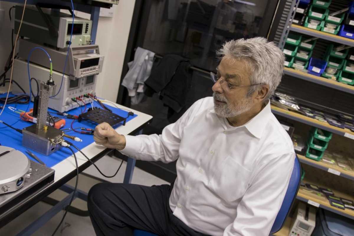
Two of Laser Components DG’s employees work full time at NanoFab, plus the company pays to support work by an ASU postdoctoral researcher. Over the years, it has boosted its business performance by refining and expanding the capabilities of its electronic detection and sensing devices through its work at the ASU facility.
The company manufactures, assembles and tests avalanche photodiodes — photodetectors based on silicon developed by the company through its work with NanoFab.
The devices are used in laser radar systems, biomedical and military applications, monitoring of ground moisture to optimize agricultural irrigation and sensing of dangerous gases for safety monitoring of mines and oil fields.
The detectors are also employed in many industrial systems and in security devices, barcode readers, range finders for distance measurements, as well as for remote temperature sensing, inspections in food packaging, sorting operations in waste recycling and in hyperspectral imaging.
Laser Components DG’s products are sold around the world, including in sizable markets throughout Asia, Australia, South America and Africa.
The Tempe-based company employs 25 people — among them physicists, chemists and electrical, mechanical, materials and software engineers.
Grubisic said the longtime mutually beneficial arrangement with NanoFab is a major factor in the company’s hard-earned success in a demanding market environment.
“We bring a need for research, ASU brings smart people, sophisticated processing and measurement equipment with extensive failure analysis capabilities. We know that by combining our knowledge and our resources, we can always get something done that will move us forward,” he said.
More companies getting on board
NanoFab has been moving forward at a record pace. In the past two years, it has seen the number of industry users increase significantly.
About 40 businesses and startups have used the facility during that time. Among them have been major tech companies such as Intel, Infineon Technologies, and ASM International. In all, close to 20 current users have longstanding projects underway at the facility.
The uptick in activity has brought a 35 percent jump in NanoFab’s revenues from business users. In addition, the number of ASU faculty members conducting research at NanoFab has jumped to more than 130.
“Everything is at its peak in users, in revenue, in user satisfaction, and in research advances,” Zhang said.
NanoFab is one of 16 facilities chosen from among more than 50 proposals from research institutions around the country to be part of the National Nanotechnology Coordinated Infrastructure (NNCI) network.
Selection as an NNCI site recognizes NanoFab as a crucial resource for nanotechnology research supporting technological innovation and commercialization critical to the nation’s economic development, said Trevor Thornton, a Fulton Schools professor of electrical engineering, the NNCI ASU site director and former longtime NanoFab director.
NanoFab’s contributions to the NNCI’s goals extend to a variety of educational outreach activities. Periodic lab tours introduce nanotechnology to K-12 students, while other programs bring university undergraduates, community college students and teachers to campus to explore nanotechnology research.
The most intensive outreach effort is a technician training program in partnership with nearby Rio Salado Community College that is aimed at preparing future workers for the nanotech industry.
That program effectively broadens NanoFab’s impact beyond directly supporting business to “developing a skilled nanotech workforce for the 21st century,” Thornton said.
Contributing to economic vitality
NanoFab’s industry partnerships and educational programs also reflect key objectives of ASU’s mission, said Sethuraman Panchanathan, ASU’s executive vice president of Knowledge Enterprise Development and chief research and innovation officer.
“We are constantly asking ourselves, ‘How can ASU be of better service to our communities and contribute to their social, economic and cultural vitality?’” Panchanathan said. “Our NanoFab core facility is one of the many offerings and services ASU makes accessible to our entrepreneurs and businesses that are advancing the economic well-being and growth of Greater Phoenix.”
Chris Camacho, president and CEO of the Greater Phoenix Economic Council, agrees.
“The reputation of Greater Phoenix as a connected place is growing, with a significant number of companies working in the internet of things and in sensor-enabled technology industries, particularly around autonomous vehicles, wearable devices, industrial automation and cybersecurity. These ventures rely on nanofabrication technologies, which remove barriers to entry for companies that are driving innovation,” Camacho said.
He views NanoFab as “an important regional asset that supports these community entrepreneurs and industry with advanced prototyping capabilities,” and as “one of the innovation centers that bridge the gap between technology development and commercialization while also driving quality job growth.”
NanoFab is seeing possibilities for its impact to grow beyond the local region, said Zhang. As one indication, he points to ASU’s selection to host an international conference last fall — sponsored by Laser Components (Laser Components DG’s parent company) — focusing on the latest advances in infrared photodetection technologies.
The event drew about 80 scientists and engineers from major research universities and industry throughout the United States, as well as from Germany, Austria and Poland.
It was the first of four of these gatherings of leading photonics and photodetection experts to be held in United States. Many of the visiting researchers took the opportunity to tour NanoFab and learn about its work.
That kind of exposure, Zhang said, is beginning to elevate NanoFab’s recognition as a productive breeding ground for nanotechnology innovation — and for helping businesses bring that innovation to the marketplace.
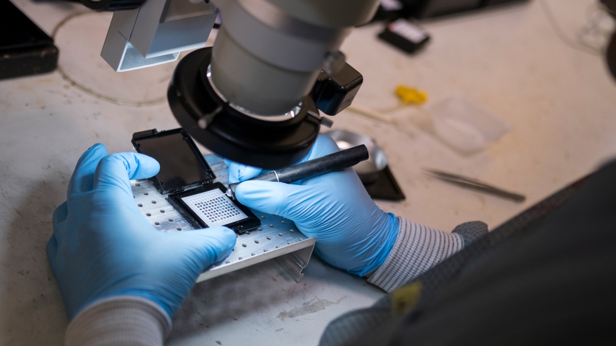
Top photo: Laser Components DG’s photodetector manufacturing, assembly and testing involve performing highly precise, intricate and meticulously controlled procedures on small, delicate components and devices. Equally complex research and development operations are done by two of the company’s employees who work at ASU’s NanoFab facility. Photo by Marco-Alexis Chaira/ASU
More Science and technology
Large-scale study reveals true impact of ASU VR lab on science education
Students at Arizona State University love the Dreamscape Learn virtual reality biology experiences, and the intense engagement it creates is leading to higher grades and more persistence for biology…

ASU-led space telescope is ready to fly
The Star Planet Activity Research CubeSat, or SPARCS, a small space telescope that will monitor the flares and sunspot activity of low-mass stars, has now passed its pre-shipment review by NASA.…

ASU at the heart of the state's revitalized microelectronics industry
A stronger local economy, more reliable technology, and a future where our computers and devices do the impossible: that’s the transformation ASU is driving through its microelectronics research…


