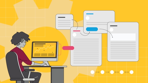
Applied Materials, ASU celebrate opening of Materials-to-Fab center to fuel microchip innovation

From left: Sandra Watson, president and CEO of the Arizona Commerce Authority; Arizona Gov. Katie Hobbs; Prabu Raja, president of Applied Materials' semiconductor products group; and Arizona State University President Michael Crow cut the ceremonial ribbon at the opening celebration of the Materials-to-Fab Center — a groundbreaking collaboration between ASU and Applied Materials Inc., supported by the Arizona Commerce Authority. The world-class shared facility for research, development and prototyping will be housed within ASU’s MacroTechnology Works building at the ASU Research Park in Tempe. Photo by Charlie Leight/ASU News
Applied Materials and Arizona State University on Thursday marked the official opening of the Materials-to-Fab Center, a shared world-class $270 million research, development and prototyping facility inside the university’s MacroTechnology Works at the ASU Research Park in Tempe.
The event was held in parallel to the SEMICON West conference in nearby Phoenix, which drew semiconductor industry leaders from around the globe.
Applied Materials executives, including Prabu Raja, president of the Semiconductor Products Group, and ASU President Michael Crow were joined at the ribbon cutting by Arizona Gov. Katie Hobbs and Sandra Watson, CEO of the Arizona Commerce Authority, along with other government and city leaders to highlight the benefits that the Materials-to-Fab Center will bring to Arizona and the entire semiconductor industry.
“The work of advancing discovery and, with it, the American semiconductor manufacturing industry is of vital importance to the nation from both an economic competitiveness and a national security perspective,” Crow said.

“The alliance between a global industry leader like Applied Materials and a leading research university like ASU, and the work that will be done in the Materials-to-Fab Center, will lead to breakthroughs and acceleration that enable chip manufacturers in the United States to lead the world in developing the technology that we need today and in the future,” he said.
The Materials-to-Fab Center will serve as a critical research and development hub for future-generation semiconductor technologies and act as a test bed for transitioning microelectronics discoveries from early-stage research to industry-ready applications — a notoriously difficult phase of development known as the “valley of death” of R & D.
The center also is designed to accelerate the transfer of innovations from ideation to fab prototype by bringing Applied Materials’ state-of-the-art semiconductor manufacturing equipment into a collaborative environment where the university, industry partners, startups, government entities and other academic institutions can work together.

“Universities are the foundation of America’s semiconductor innovation pipeline, and we look forward to bringing together ASU’s world-class engineering teams with Applied Materials technologists and ecosystem partners at the Materials-to-Fab Center," Raja said. "These collaborations will focus on accelerating development of new chip technologies that are crucial to U.S. leadership in AI, high-performance computing and other megatrends shaping the future.”
Applied Materials is the largest U.S. supplier of semiconductor manufacturing equipment. Its tools are used to produce virtually every new chip in the world. ASU complements that leadership by conducting research in areas from front-end innovation to advanced packaging and large-scale manufacturing, and — with the nation’s largest engineering school with nearly 33,000 students — is a driving force behind the workforce and talent development that is critical to the industry’s future.
“The Materials-to-Fab Center is a marriage made for Arizona and something that will benefit the entire region,” Hobbs said. “Applied Materials is an industry leader that already has a presence in the state with many of its customers invested in doing work within the ecosystem that is growing here, and Arizona State University is a powerful force behind all the work being done, producing both the people who will lead this industry into the future and the ideas that will shape its progress.
"I am grateful to the Arizona Commerce Authority for helping this all come together and very excited to see this contribution to our economy coming to realization.”
Watson described the opening as a win for the state.
“The launch of the Materials-To-Fab Center ushers in a new era for U.S. semiconductor innovation, providing a one-of-a-kind platform where innovators can test, refine and accelerate new processes and technologies,” she said. “This pioneering collaboration between Applied Materials and ASU strengthens Arizona’s position as a national leader in semiconductor R & D, and we’re proud to support this transformative initiative.”
The Materials-To-Fab Center builds on Applied Materials’ existing presence at ASU’s MacroTechnology Works facility, as well as the research already being funded by the company involving ASU faculty and students.
This longstanding collaboration has laid the groundwork for projects awarded to ASU through the CHIPS and Science Act for the Southwest Advanced Prototyping, or SWAP, Hub, which is advancing rapid translation of technologies for national defense, as well as the SHIELD USA project, which is focused on advanced packaging technologies.
“The physical space that this delivers and the tools provided by Applied Materials through this alliance are a very important part of the Materials-to-Fab Center,” said Sally Morton, executive vice president of ASU’s Knowledge Enterprise, which leads research for the university. “But it’s also a place for the experts in this field, ASU faculty and industry leaders to come together and share ideas. Applied Materials is bringing the voice of the customer, and ASU is adding the curiosity and creativity of its students. We’re very excited about what will happen here.”
-

Sally Morton, the executive vice president of ASU’s Knowledge Enterprise, emcees at the grand opening of the Materials-to-Fab Center on Oct. 9.
Photo by Charlie Leight/ASU News
-

Arizona Gov. Katie Hobbs speaks at the opening event for the Materials-to-Fab Center at the ASU Research Park in Tempe on Oct. 9.
Photo by Charlie Leight/ASU News
-

Kyle Squires (center), dean of the Ira A. Fulton Schools of Engineering, speaks with attendees at the opening event for the Materials-to-Fab Center at the ASU Research Park in Tempe on Oct. 9.
Photo by Charlie Leight/ASU News
The Materials-To-Fab Center will be an asset to small and large companies across the state and the Southwest region, and a key capability for connecting ongoing investments in research and manufacturing.
“We’re taking technologies from the early discovery phase to the point where they’re ready for real-world use,” said Seth Ariel Tongay, a professor in the School for Engineering of Matter, Transport and Energy who has conducted research in the Materials-To-Fab Center. “That’s the stage where many great ideas tend to stall. This center is designed to make sure they don’t.”
Tongay’s work in the center focuses on a fascinating new class of materials known as two-dimensional, or 2D, semiconductors. These materials are just a few atoms thick, or so thin they’re essentially flat. They hold enormous promise for powering the next generation of technologies, from lightning-fast AI processors to cutting-edge quantum devices.
But developing these materials and turning them into usable technology are two very different things, and that’s where the Materials-To-Fab Center stands apart. The combination of university-led scientific research, industrial-grade manufacturing equipment and tools typically found only in top-tier commercial fabs — allowing a full-stack capability, from synthesis to testing to prototyping, all under one roof — empowers researchers to rapidly iterate and refine their ideas in ways that are directly aligned with what industry actually needs.
“This kind of setup is almost unheard of in a university setting,” Tongay said. “Most research labs stop at discovery. The MTF Center lets us go further. We can take those discoveries and develop them into real, manufacturable technologies.”
Kelly deVos and Jay Thorne contributed to this story.
More Science and technology
When facts aren’t enough
In the age of viral headlines and endless scrolling, misinformation travels faster than the truth. Even careful readers can be swayed by stories that sound factual but twist logic in subtle ways that…
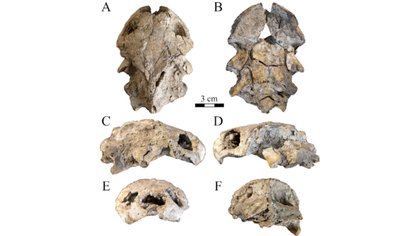
Scientists discover new turtle that lived alongside 'Lucy' species
Shell pieces and a rare skull of a 3-million-year-old freshwater turtle are providing scientists at Arizona State University with new insight into what the environment was like when Australopithecus…

ASU named one of the world’s top universities for interdisciplinary science
Arizona State University has an ambitious goal: to become the world’s leading global center for interdisciplinary research, discovery and development by 2030.This week, the university moved…