Scaling down manufacturing dimensions to scale up chip production

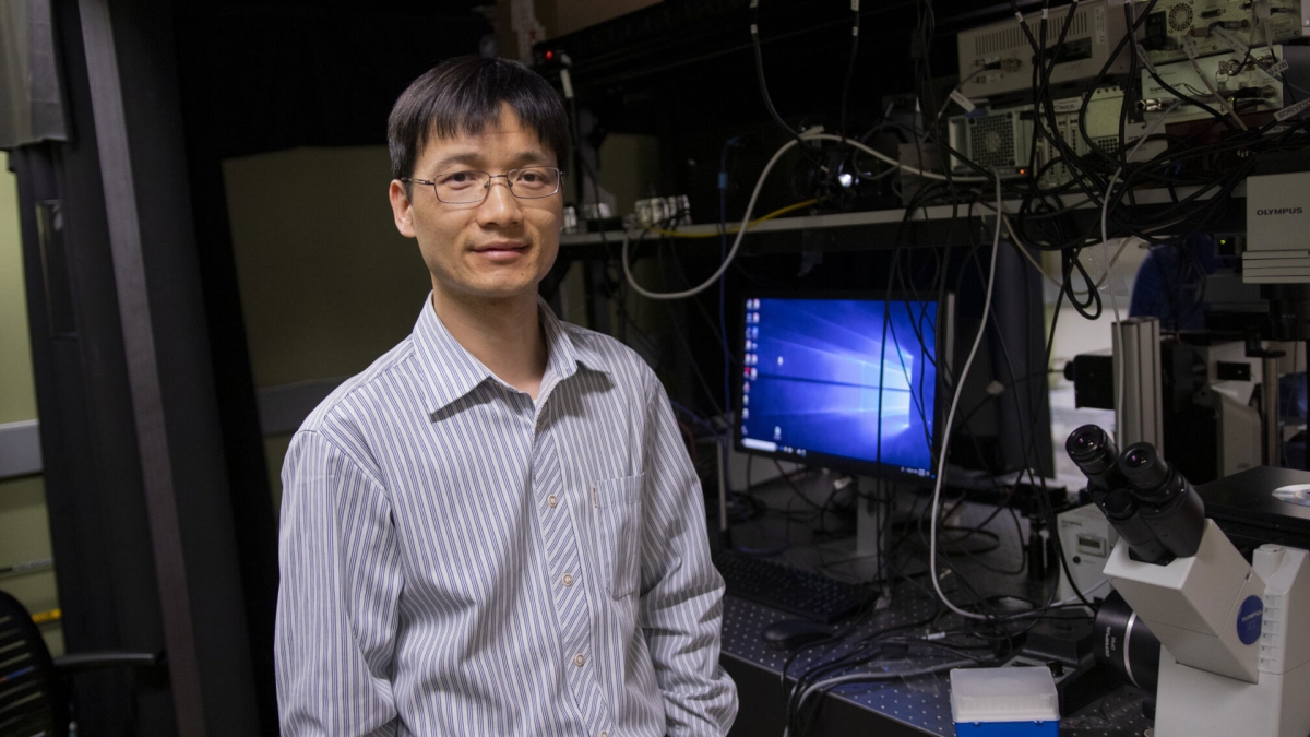
Chao Wang, an electrical engineering researcher in the Ira A. Fulton Schools of Engineering at Arizona State University, is developing an accessible manufacturing method for researchers to prototype and fabricate their designs. Photo by Marco Alexis-Chaira/ASU
Devices that once took up whole rooms can now be carried in one hand. Smaller, cheaper and superior designs are the benchmarks of progress. Fueling this race of breakthroughs are the continuous efforts to miniaturize semiconductor chips. While electronics have enjoyed great success, achieving the same advancements has been challenging for optical devices, such as camera lenses.
This can all be changed using metasurfaces, which are thin structures nanoengineered to have unique optical properties based on the material they are made of, as well as their structural geometries. Such metasurface structures, in principle, can be fabricated in semiconductor factories that make the most advanced silicon chips.
However, in practice, these processes are expensive, time-consuming and difficult to access for small-scale exploratory projects or prototyping, leaving many novel theories untested.
Chao Wang, an associate professor of electrical engineering in the School of Electrical, Computer and Energy Engineering, part of the Ira A. Fulton Schools of Engineering at Arizona State University, and associate faculty member of the Biodesign Center for Molecular Design and Biomimetics, developed a scalable multilayered manufacturing approach with nanoimprint lithography for researchers to prototype and produce metasurfaces in ultracompact devices.
“Researchers at universities need an established and accessible method for manufacturing metasurface products precisely over nanometer scale and, at the same time, produce them over millimeter scale or larger,” he says.
Waffle-making at a nanometer scale
The rate at which researchers are theorizing is outpacing available resources, so Wang set out to design a tool to sustain the pipeline between idea and tangible product.
“For many electronic or photonic devices, they require multiple layers of materials to perform their function,” Wang says. “Only a few foundries in the world have access to the tools to make this; most university researchers don’t have access.”
A recent paper published in the scientific journal Advanced Functional Materials titled “Scalable Nanoimprint Manufacturing of Functional Multilayer Metasurface Devices” revealed the findings by Wang’s team.
They began by revisiting the printing method, known as nanolithography, which prints features on the chip within a nanometer of precision, to enable functions. The most common method is electron-beam lithography, which can only fire one beam on a small surface at a time. Wang chose to use nanoimprint lithography, or NIL, which produces results quickly over a larger area.
“NIL is like making a waffle,” Wang says. “The batter is turned into a waffle with the textures replicated from the waffle maker. With the right batter and waffle maker, you can make waffles at a size you want in a short amount of time and repeat that again and again.”
Perfect alignment comes from imperfection
NIL has been adopted in recent years for different semiconductor processing applications, from electronic to photonic devices, including metasurface structures. However, there are so far no successful demonstrations of fabricating multilayer metasurface structures, which provide significant design freedom for enhanced functionalities.
To perfectly align multilayer structures, Wang’s team utilized a technique called moiré patterns, which happen when two very similar, but not identical, arrays of lines are overlaid. The technique can be experienced by aligning two similar combs and moving one slightly to observe periodic dark and bright patterns formed behind the teeth.
This exact concept was explored by the researchers to produce interference patterns of intentionally designed moiré alignment marks that allow them to sensitively detect nanometer-scale alignment errors with their bare eyes. To make this work, the NIL molds — or the waffle irons in Wang’s metaphor — for both metasurface layers need to be engraved with the moiré marks, and the second NIL mold needs to be optically transparent so that the researchers can adjust alignment during the NIL process.
Smart 3D scaffold simplifies manufacturing
Nanofabrication is usually a complex process, involving multiple steps of thin film deposition, pattern formation and material removal. Going through all the steps on an existing, bottom-layer metasurface structure inevitably adds risks of structural damage. To simplify this, the researchers in Wang’s lab innovated a 3D scaffold concept for the top-layer metasurface structure.
“In the conventional fabrication, one may carve out carefully the pockets in the waffle, put the waffle on a plate, spray chocolate through the holes, toss away the waffle, and serve only the chocolate remaining on the plate,” Wang says. “Now what we do is carefully paint the chocolate both on top of the grid and in the pockets, and serve the chocolate-topped waffle as is.”
The 3D scaffold concept allows researchers to build novel metasurfaces vertically, drastically reducing the time and cost of prototyping sophisticated devices. Wang describes the process as a series of co-designing decisions, ultimately turning a 24-hour process into a matter of minutes, surpassing major hurdles for manufacturing.
“Essentially, we designed a new waffle iron, new batter and the right conditions to spray chocolate,” he says.
Reimagining imaging
Wang tested the manufacturing method’s precision and alignment with collaborator Yu Yao, an associate professor of electrical engineering in the Fulton Schools who received the National Science Foundation Faculty Early Career Development Program (CAREER) Award in 2021 to reimagine the polarimetric microscope.
Yao’s microscope was the ideal test for the manufacturing method due to the need for metasurfaces with high-resolution printing yet precisely aligned to support the sensor. The new method helped condense the microscope’s analyzer from the size of a microwave to a microscopic chip.
Yao says scalable nanomanufacturing of nanophotonic structures and metasurfaces is essential for technology transfers from lab to commercial applications.
“So far, most researchers in the field have been using fabrication methods with costs that outweigh applications,” Yao says. “The NIL manufacturing method provides a fast and economical solution for fabrication and can be readily extended to large-scale production of various devices and systems, greatly shortening the time from lab demonstration to commercial product.”
Applications and future implications
Wang is eager to have researchers adopt his manufacturing method and see the ideas that will be prototyped.
“It is fulfilling for us to prove that these processes can work and are scalable,” Wang says. “It’s not limited to one thing and has generalizable platform technology that can impact many different fields.”
Alongside prototyping, production and novel optical applications, he foresees the technology being advantageous for printing, imaging and information processing.
He hopes his method can help sustain the microelectronics demand from energy, defense and medical device industries.
“We plan to explore how these processes can be used for advancing semiconductor electronic devices,” Wang says. “This research provided a preliminary demonstration of what is feasible, and we anticipate more interesting things to come.”
Wang is preparing to explore broad applications for semiconductor electronics and photonic integration through the National Science Foundation and the Department of Defense.
“The metasurface field is exploding,” Wang says. “People see the need to produce photonic structures in semiconductor technology, ultimately beating out the conventional optical devices that are big and bulky.”
More Science and technology

ASU travel behavior research center provides insights on the future of transportation
The Center for Teaching Old Models New Tricks, known as TOMNET, has spent the past seven years conducting research and developing tools to improve transportation systems planning methods and data.As…

When suspect lineups go wrong
It is one of the most famous cases of eyewitness misidentification.In 1984, Jennifer Thompson was raped at knifepoint by a man who broke into her apartment. During the assault, she tried to make a…

Jackpot! ASU hackers win $2M at Vegas AI competition
This August, a motley assortment of approximately 30,000 attendees, including some of the best cybersecurity professionals, expert programmers and officials from top government agencies packed the…