MacroTechnology Works collaborations spark industry innovation

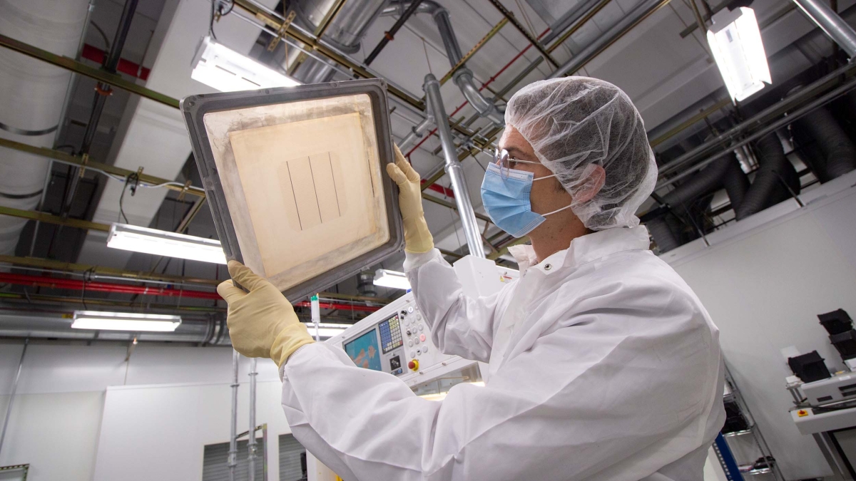
MacroTechnology Works, or MTW, is a new Arizona State University facility where industry members working in semiconductor, microelectronics and associated fields get a combination of access to advanced equipment and research capabilities that, to date, only exist at ASU. Photo: ASU
Semiconductors power the products we use every day, from cars to smartphones to household appliances. Microelectronics is a term used in the industry to include computer chips integrated with other components.
The Phoenix metropolitan area has increasingly become known for the long-standing and growing presence of semiconductor and microelectronics companies. Now, some of these companies are finding their homes at MacroTechnology Works, or MTW, a new Arizona State University facility where industry members working in these and associated fields get a combination of access to advanced equipment and research capabilities that, to date, only exist at ASU.
Arizona U.S. Sen. Mark Kelly notes that the facility offers a unique environment for companies looking to make their mark in microelectronics and semiconductor device manufacturing in the state.
“I’ve seen Arizona State University’s state-of-the-art MacroTechnology facility up close,” Kelly says. “Their work to integrate research, development and manufacturing is a game-changer for our state. Thanks to investments from our CHIPS Act and leadership at ASU, this facility will make sure we have the robust workforce, from engineers to researchers, needed to support Arizona’s growing semiconductor industry."
Private companies can lease space in MTW from a few hundred to several thousand square feet in the one-of-a-kind research facility. Through research partnerships with ASU, they can collaborate with faculty and students to accelerate semiconductor, advanced materials and energy device research.
“MacroTechnology Works has the scale and sophistication of an industry semiconductor fab capable of running state-of-the-art processes and materials at the wafer or substrate scale of industry with the flexibility of academia,” says Zachary Holman, an associate professor of electrical engineering in the Ira A. Fulton Schools of Engineering. “We have equipment for the scale of manufacturing production, but instead of being used for manufacturing, it’s being used for research and development.”
A distinct opportunity for research
What distinguishes MTW from other spaces is the type of research conducted there. MTW enables a faster way to get products to market by eliminating extra steps in the development process. Instead of first testing experimental microelectronic devices on a smaller scale and then taking further development time to build larger versions of the devices for production, experimental devices can be built on the same scale at which they will be produced.
Along with gaining access to more efficient research capabilities, tenants in MTW effectively become research partners with ASU, complete with sponsored research agreements.
“When companies come to MTW, it’s not just about the space,” Holman says. “It’s about the connections, the people, the research projects and engagement with graduate and undergraduate students.”
MTW also has the chemicals and associated piping and storage required to conduct this complex electronics research, which he says can be costly to add to an existing building.
When Holman and his former doctoral student Peter Firth looked for lab space to rent for Swift Coat, a company the pair founded that makes coatings for surfaces that can help reduce reflection, prevent dirt accumulation and increase adhesion, they discovered that installing the needed infrastructure in a warehouse would have cost several million dollars. Holman also estimates that moving into MTW saved the company six months to a year that would have been needed to set up the infrastructure in an unequipped space, helping Swift Coat get started faster.
After renting a 500-square-foot space in MTW for three years and raising $10 million in investments, Swift Coat has grown large enough that it will soon be relocating to a 16,000-square-foot facility in Phoenix.
“This is a success story; it’s exactly what should happen,” Holman says. “You get big enough that it makes sense to go build your own facilities and grow out of MTW. But that transition period from small to large, between the two, is exactly where MTW is the perfect fit and a huge enabler.”
These successes have attracted national political attention.
During a visit to MTW last fall, U.S. Secretary of Commerce Gina Raimondo says the work being done at ASU to develop partnerships and invest in student success is something that “every public university in the country should be doing.”
The Department of Commerce, she says, is committed to training a diverse workforce that is prepared to take on roles in the semiconductor sector and create a nationally competitive environment where states like Arizona can continue to advance in this field.
“It is my mission — my obsession — at the Commerce Department to help America compete, to enhance America’s competitiveness in the world,” says Raimondo. “And enhancing America’s competitiveness in the world begins right here in buildings just like this, which is to say the basic research and development money from the government coming together with business — from the biggest to the smallest — with academics, solving the problems of today and tomorrow.”
Similarly, Heidi Shyu, undersecretary of defense for research and engineering at the U.S. Department of Defense, praised MTW for the opportunities through which it allows businesses to collaborate with academic experts and use its advanced facilities.
“The fact we can tap into an incredible ecosystem right here is so impressive,” Shyu says. “The facility I just walked through, which allows small startups as well as faculty to tap into it, will be a major benefit.”

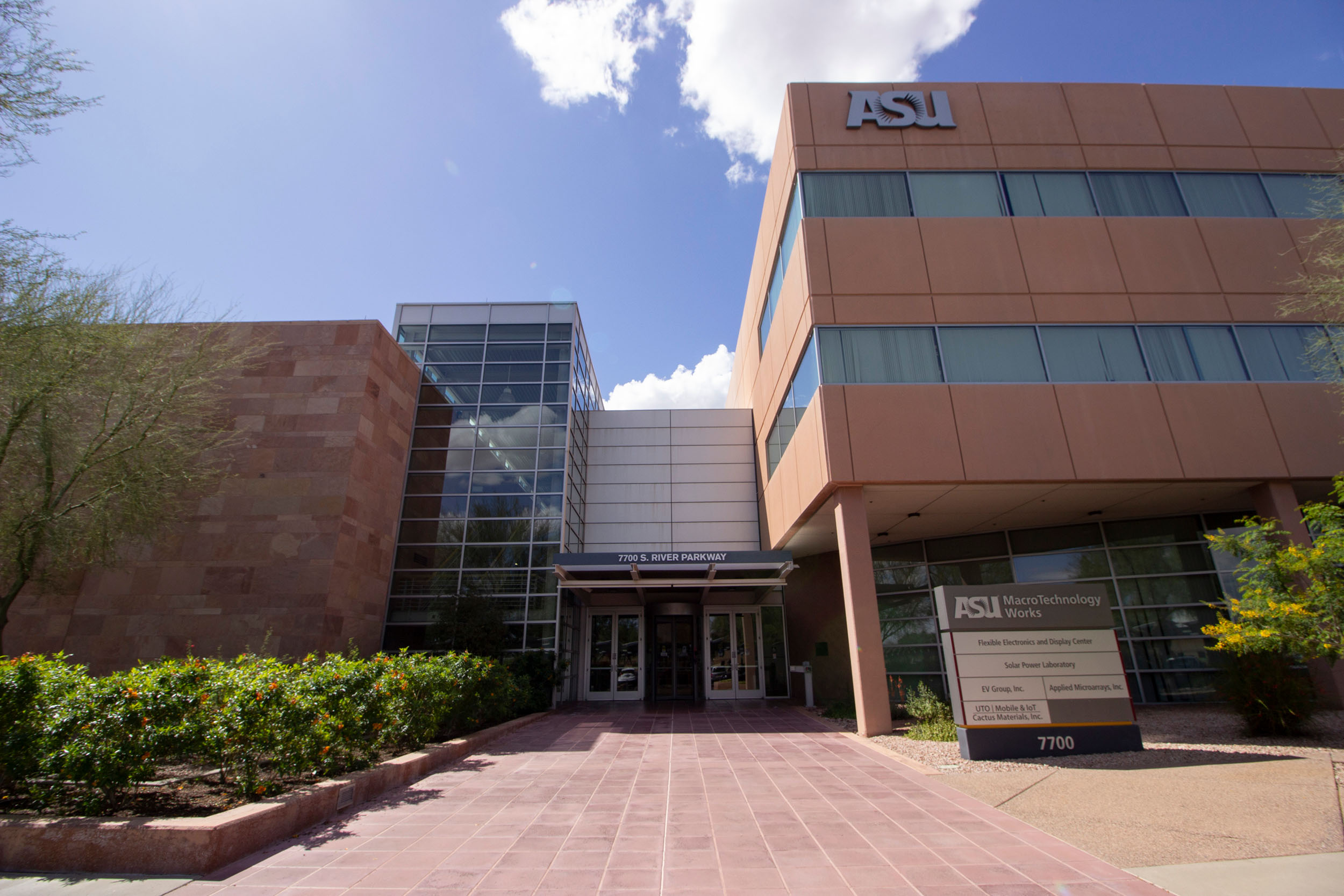
MacroTechnology Works was originally a Motorola semiconductor fabrication plant when it was constructed in 1997. ASU has owned the building since 2004. Photo by Erika Gronek/ASU
An incubator for revolutionary research in electronics
Currently, there are 10 companies leasing space in MTW. They include semiconductor equipment manufacturers and device-makers, solar cell and panel manufacturers and battery technology developers. Among them are Applied Materials, Cactus Materials, Atomera and Advent Diamond.
Scott Bibaud, president and CEO of Atomera, which designs a film that helps semiconductor materials move electrons faster and leases space in MTW, agrees with Holman that the people in the facility are a valuable asset for business, even beyond students and faculty members.
“It’s kind of an ecosystem of companies like us that are doing material research in advanced areas,” Bibaud says. “Just being in this environment of innovative companies and talking to people from them in the hallway is helpful.”
Other companies in MTW don’t lease on-site space but instead conduct research in the ASU Core Facilities at MTW, which offer capabilities to make prototypes or conduct testing of electronic devices, including solar panels.
“These companies might, for example, use one of our two Core Facilities at MTW, Advanced Electronics and Photonics and the Solar Fab, to make prototypes or do certain tests on their behalf,” Holman says. “They’re paying for that service, but it’s not their engineers doing the testing, and they’re not necessarily located in Arizona.”
A prominent research collaboration between ASU researchers and Northrop Grumman Mission Systems includes the use of diamond as a semiconductor material for potential applications to make electric vehicle charging and communication technologies run faster than what is possible using silicon, the traditional computer chip material.
Solestial, a startup company in MTW, is developing new solar technology for spacecraft that will cut the cost of solar panels used in space by 90% compared with traditional solar panels. ASU electrical engineering doctoral alumnus Stanislau Herasimenka founded the company, which recently raised $10 million in a seed funding round by Airbus Ventures.
Kevin Reinhart, the executive director of research project management at ASU who manages the MTW facilities, says that MTW wants to attract industry partners that will use the building’s space for its distinct capabilities. He sees these collaborations between ASU and industry partners as mutually beneficial.
“While our faculty researchers now have a project, and that becomes a focus for students who are gaining knowledge from their research experience,” he says, “they’re producing research papers and other outputs that can go to industry more broadly. Ultimately, industry is essentially being given answers to their specific problems, and they’re getting a better trained workforce.”
Much of the work happening in MTW also supports the New Economy Initiative, a statewide initiative to advance high-tech industries in Arizona. Research in the Advanced Materials, Processes, and Energy Devices Science and Technology Center, or AMPED STC, connects industry partners and governmental entities with ASU faculty researchers to create the materials and devices needed for broad electrification of the energy sector.
A long history in the Phoenix microelectronics landscape
Originally built by Motorola in 1997, the Tempe building was part of the company’s flat panel display prototype manufacturing, which was also once headquartered at the site. It features 43,500 square feet of cleanroom space, which minimizes environmental hazards that can affect sensitive materials used for electronics research, development and manufacturing. The facility also includes H6 capability, meaning it provides infrastructure for chemicals required for semiconductor production.
ASU purchased the building from Motorola in 2004 when the company phased out its Arizona semiconductor manufacturing activities. The university had just secured a grant from the U.S. Army to form the ASU Flexible Electronics and Display Center, which focused on flexible screen development. Given the building’s recent history with Motorola, it was suitably outfitted to be the center’s new home.
The site later played host to Quantum Energy and Sustainable Solar Technologies, an ASU-led National Science Foundation Engineering Research Center focused on developing solar power and sustainable electricity generation technology. The center was funded by the NSF from 2011 until 2021.
While the projects in those two centers have been successfully completed, MTW continues to support a vibrant array of electronics research for both ASU investigators and industry partners who rent space in the facility.
MacroTechnology Works’ growth over the years
1997: Motorola builds the facility that would later become MacroTechnology Works.
2004: ASU buys MacroTechnology Works from Motorola and establishes the Flexible Electronics and Display Center.
2009: Solar Power Lab is established and produces its first silicon solar cells one year later.
2011: Quantum Energy and Sustainable Solar Technologies is established.
2013: Solar panel arrays are installed to generate sustainable electricity.
2019: Semiconductor company Applied Materials, which had $25.8 billion in revenue in 2022, leases space in MacroTechnology Works.
2020: The Flexible Electronics and Display Center transitions to become ASU’s Advanced Electronics and Photonics core facility.
2021: The former Quantum Energy and Sustainable Solar Technologies lab space transitions to become ASU’s Solar Fab core facility.
To inquire about leasing space in MacroTechnology Works, contact Kevin Reinhart at kevin.reinhart@asu.edu.
More Science and technology

ASU professor honored with prestigious award for being a cybersecurity trailblazer
At first, he thought it was a drill.On Sept. 11, 2001, Gail-Joon Ahn sat in a conference room in Fort Meade, Maryland.…

Training stellar students to secure semiconductors
In the wetlands of King’s Bay, Georgia, the sail of a nuclear-powered Trident II Submarine laden with sophisticated computer…

ASU startup Crystal Sonic wins Natcast pitch competition
Crystal Sonic, an Arizona State University startup, won first place and $25,000 at the 2024 Natcast Startup Pitch Competition at…