image title

ASU's role in boosting state's semiconductor initiative years in the making

ASU's role in semiconductor industry boost has been years in the making.
January 17, 2023

University involved in workforce education, bridging the 'lab to fab' gap

While the CHIPS and Science Act was signed into law less than six months ago, releasing $52 billion over five years for a push to improve national security technology, Arizona State University has been working to prepare for this opportunity.

Grace O’Sullivan, vice president of corporate engagement and strategic partnerships for ASU’s Knowledge Enterprise, said that the university began thinking about its role in researching and developing semiconductor manufacturing five years ago, working with many partners along the way.

“It’s an interdisciplinary effort to make all of this work between government agencies, universities and community colleges, and these things don’t happen overnight,” she said during a webinar on Friday about the CHIPS Act, sponsored by the Morrison Institute for Public Policy at ASU. She was joined on the webinar by Sean Fogarty, vice president of international business development for the Greater Phoenix Economic Council.

“GPEC and ASU, under the vision of ASU President Michael Crow, have been planning this for years.”

RELATED: More microelectronics news out of ASU

Arizona is going to be a major player in this initiative, thanks to a monumental investment by the Taiwan Semiconductor Manufacturing Company (TSMC), which is building two gigantic chip-fabricating centers in north Phoenix.

“TSMC said they chose Arizona because of the cooperation between public and private entities, and we were proud of that and continue to work as a team,” O’Sullivan said. She was part of a state team that visited Taiwan three years ago during the pitch to attract the company here.

Part of Arizona’s preparation to build up America’s semiconductor capacity is the New Economy Initiative, a massive collaboration among the state’s three public universities, private companies and state government to bring Arizona to the frontier of high-tech industry.

Funded by the state, the New Economy Initiative’s goals are to create 40,000 new high-wage jobs by 2041, increase economic output to $6.9 billion by 2032 and double the return on the state’s investment by the same year.

ASU will be a major player in several ways, including workforce development, increasing the number of engineers and in bridging the critical “lab to fab” gap — the time lag between when technology is invented and when it’s ready to be fabricated and put into use.

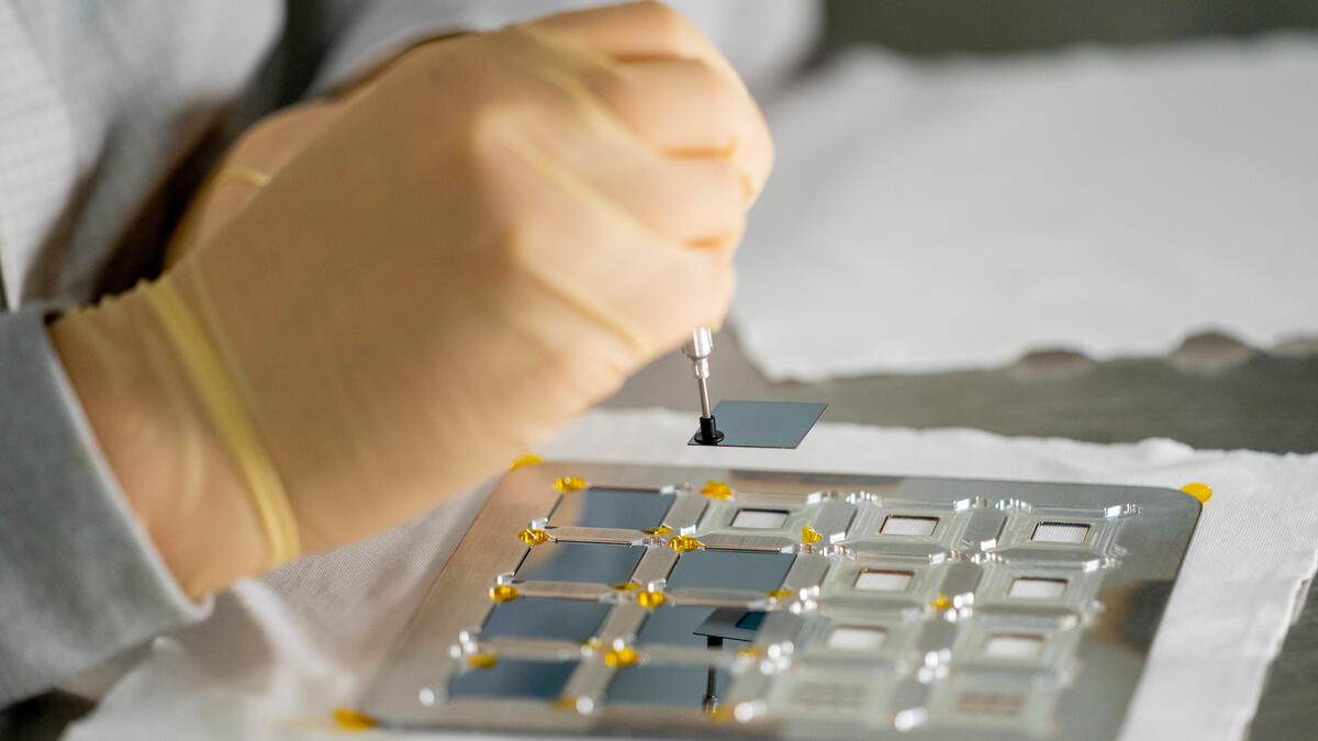
One important component to that will be ASU’s MacroTechnology Works in Tempe, a unique lab and fabrication space that is open to both university researchers and community partners, from tiny ventures to big corporations.

“We’ve had a strong history in Arizona when Motorola opened its fabrication here in the 1950s. ASU acquired that fab and renovated it into the MacroTechnology Works in ASU’s research park,” O’Sullivan said, adding that the U.S. imports more than 90% of the microchips it uses.

“U.S. manufacturing capacity has eroded from 37% of the market to 12% today,” she said.

“A lot of it was because it was cheaper to make things overseas, and also the U.S. didn’t invest as heavily in these industries with incentives as much as countries in Asia did.

“We’re now trying to capture the moment on how Arizona is becoming ‘Semiconductor Central.’”

Fogarty said that Taiwan Semiconductor’s $40 billion investment is one of the largest foreign direct investments in U.S. history and will create a massive ripple effect in everything from shopping to K–12 education.

“It will create 4,500 high-wage jobs, lead to over 21,000 construction jobs and over 13,000 jobs at supplier companies,” he said.

Since July, the Greater Phoenix Economic Council has helped 22 companies relocate here, bringing 4,800 jobs.

Fogarty said the plants will have a lot of jobs that don’t require a bachelor’s degrees.

“For every engineer TSMC has on staff, they probably need four to six technicians,” he said, noting that the community colleges have started to offer “boot camps” for those jobs.

The goal is economic mobility, he said.

“It’s not just PhDs and masters and bachelors we need. It’s also high school-leavers we’re hoping to help, and people in other industries who can be reskilled to take on these high-wage jobs,” he said.

ASU has leveraged its expertise at several points along this multiyear initiative, O’Sullivan said, from having faculty involved in drafting parts of the legislation to having the Kyl Center for Water Policy advise local leaders on water use by semiconductor manufacturers.

“We were just visiting with TSMC this morning to talk about talent needs,” she said.

“We want to be that epicenter of innovation and design, bringing all of our assets.”

Top image: A researcher works at the ASU MacroTechnology Works lab and fabrication space in Tempe. Photo by Samantha Chow/ASU News

Mary Beth Faller

Reporter , ASU News

480-727-4503

 
image title

Workshop brings academic, industry partners together to collaborate on CHIPS Act projects

July 27, 2023

ASU's SWAP Hub aims to position Southwest as a semiconductor epicenter

In the global race to lead on microchip manufacturing, research and development, Arizona State University — in anticipation of opportunities that will come from its CHIPS and Science Act proposals and partnerships — is already beginning to plan, collaborate and produce. 

Last week, the university held a workshop with more than 30 partners from academia, industry, national laboratories and nonprofits to discuss four quick-turn projects that will showcase the team’s readiness for national defense programs funded by the 2022 CHIPS and Science Act.

ASU has been preparing for years for the influx of work necessary to boost national security technology. In February, ASU submitted a proposal for a strategic public-private partnership on cutting-edge research and development to speed the transformation of ideas generated in the lab into practical solutions.

That collaborative effort, known as the Southwest Advanced Prototyping Hub, or the SWAP Hub, is led by ASU and has more than 60 leading corporate, startup, academic and national lab partners from the semiconductor and defense sectors in Arizona, New Mexico, Colorado and beyond.

Video by Ken Fagan/ASU News

The SWAP Hub was proposed for consideration as part of the Microelectronics Commons, a $1.63 billion Department of Defense program funded by the 2022 CHIPS and Science Act.

Sally Morton, executive vice president of ASU’s Knowledge Enterprise, told partners assembled at the workshop that the Department of Defense is now evaluating the hub proposals and is expected to announce the funding awards before the end of federal fiscal year at the end of September.

“But we have not waited idly for their response. Just the opposite,” she told the workshop participants.

“The Southwest is already one of the nation’s key centers for microelectronics activity. It’s home to some of the leading semiconductor producers and suppliers, major defense contractors, world-class universities and research institutes, and a vibrant startup community,” she said.

RELATED: Prototyping facility will give students, startups access to semiconductor space

Zachary Holman, associate professor in the School of Electrical, Computer, and Energy Engineering at ASU, told the SWAP Hub collaborators that ASU is funding four seed projects at $50,000 each, with the expectation that partners on the projects will match that funding.

“We want to get projects going within the SWAP Hub even before the government decides whether the SWAP Hub should exist,” said Holman, who also is director of faculty entrepreneurship within the Ira A. Fulton Schools of Engineering.

“We would like teams comprising folks in this room, and folks not in this room, to have already been working together for months to have initial results that can parlay into much larger projects.”

ASU is accepting proposals with an Aug. 11 deadline for the projects, which will be six months in duration and will provide proof-of-concept that the SWAP Hub is ready to move quickly on much larger-scale work.

The projects will fall within three specific areas: 5G/6G technology; artificial intelligence hardware; or “commercial leap-ahead technology,” which includes new materials and other technologies that can quickly move the U.S. military beyond traditional weapon platforms like tanks, helicopters and gunships.

Each team that proposes a project must have at least one ASU principal investigator and at least one SWAP Hub member. Each project must show how it can be scaled up.

There are two main goals of the hub program, according to Kevin McGinnis, managing director of strategic technology initiatives at ASU: improve the “lab-to-fab” pathway – the ability to take an idea in the lab and transition it to a usable outcome — and develop a prepared workforce.

“We have the opportunity with this team to move ideas through university labs and startup companies and, with the help of our defense partners, place them onto defense platforms,” he said.

“We want to take ideas that happen here in the Southwest from a prototype stage all the way through to commercial fabrication and ideally onto a national defense platform that has high impact.”

The SWAP Hub also will provide access to cutting-edge technology to students, even undergraduates.

“We hear about workforce development needs every day,” McGinnis said.

“It seems that especially in the Department of Defense, where there are special requirements related to U.S. citizenship, that their pool of qualified workers is small and diminishing, so we need to offer a number of pathways to move people into the DoD microelectronics ecosystem, whether that’s at a national lab, a defense contractor, or the DoD itself.”

Several ASU students are part of a pilot internship program at Sandia National Laboratories, according to Ken Dean, senior manager of Advanced Semiconductor Technologies at Sandia.

As a Department of Energy National Laboratory, Sandia performs fundamental research and basic science, and develops national security technology for the U.S. This includes operating a production-rigor semiconductor fabrication facility.  

“Students can work with our semiconductor equipment and get exposure to both research topics and high-rigor production processes,” Dean told the gathering on Friday.

"The benefit to having interns here is we can start security clearances for them while they’re in the intern program, thereby creating a national security workforce that is ready to go.” 

Top photo: Rafi Islam, CEO and CTO of Cactus Materials Inc. in Tempe networks with others at the Southwest Advanced Prototyping Hub Workshop on July 21 at SkySong, the ASU Scottsdale Innovation Center. The objective of the daylong conference was to prepare ASU and its partners to rapidly develop projects related to the DoD Microelectronics Commons for execution under the SWAP Hub, in cooperation with other regional hubs. ASU also announced an offer of four $50,000 grants in seed funding to kick-start SWAP Hub-related projects. Photo by Charlie Leight/ASU News

Mary Beth Faller

Reporter , ASU News

480-727-4503