Alaskan coast 8.2 magnitude earthquake recorded by ASU seismometer


July 29, 2021

The 8.2 magnitude earthquake that struck off Alaska’s coast on July 28 was the strongest earthquake in the area since 1964 and generated tsunami warnings for the coastal areas of south Alaska, the Alaska Peninsula, and the Aleutian Islands. According to the U.S. Geological Survey (USGS), the strong quake was located about 56 miles (90 kilometers) east-southeast of Perryville, Alaska, and was 29 miles (46.7 km) deep. Earthquakes are known to occur at any depth from right at the Earth's surface to approximately 430 miles (700 km) down.

While the tsunami is no longer a threat, seismometers all over the world recorded this quake, including one located in the basement of a building on the Arizona State University Tempe campus. The data on the quake is displayed on a new ASU website: earthquake.asu.edu. Close-up of the Guralp CMG-3T broadband seismometer, topped with the Guralp DM-24 signal digitizer. Keys are included for scale. The digital signals from this combination are recorded on a nearby desktop PC. Credit: West/ASU Download Full Image

More: ASU-recorded data on earthquakes 

This seismometer and corresponding website are managed by ASU geophysicists John West and Edward Garnero of the School of Earth and Space Exploration. The public site provides information on earthquakes and seismic activity from anywhere in the world as measured at ASU, compiling earthquake information provided by the USGS, including magnitude, latitude, longitude and depth, and then calculating the distance of the earthquake from ASU.

“The ASU seismometer was set up as a reference instrument to support our long-running series of projects to develop a planetary exploration seismometer for NASA,” said West. “Once it was set up and recording full time, it made sense to make the output available to the public.”

Seismometers are designed to be sensitive to the motions of the Earth and can detect earthquakes, volcanic eruptions and explosions. The ASU seismometer is a broadband Guralp model CMG-3T sensor and includes three weights suspended by precision springs.

When the ground moves from an earthquake, the seismometer case moves with the ground motion but the suspended weights, by inertia, initially do not. The seismometer then records the motion of the instrument around the weights in north-south, east-west and up-down directions.

“This is a very sensitive instrument,” said West. “It can record a motion as small as one-fiftieth the diameter of a human hair.”

The ASU seismometer is located in the basement of the Bateman Physical Sciences Building F-Wing on the ASU Tempe campus, which was specifically designed to accommodate a seismometer. Builders installed a vertical concrete column projecting 40 feet into the subsurface below the basement and equipped the column with rubber gaskets to help isolate it from building vibrations so the seismometer could more distinctly measure vibrations from earthquakes.

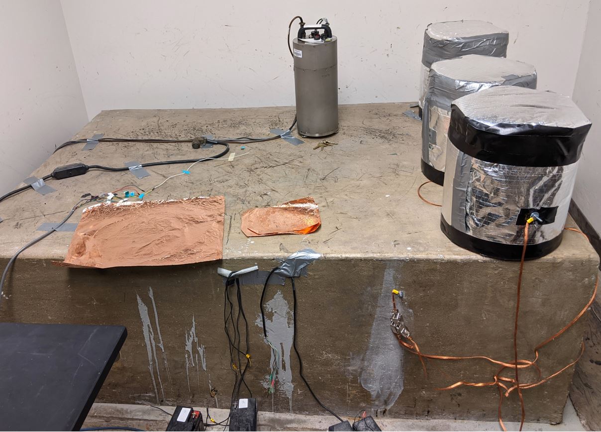
The Guralp seismometer on the concrete seismic pier in the basement of Bateman Physical Sciences building F-wing. The pier is vibrationally isolated from the building and extends approximately 40 feet below the basement floor. Canisters on the right provide electromagnetic and thermal isolation for testing new sensors. Credit: West/ASU

“Our seismometer provides information on how earthquakes register in Tempe specifically,” said West. “We intend to provide a local view of these global events.” 

In addition to information on the most recent earthquakes, visitors to the website can also learn about historical earthquakes and fault locations in Arizona and sign up for earthquake e-mail alerts on newly detected and plotted earthquakes.  

Karin Valentine

Media Relations & Marketing manager, School of Earth and Space Exploration

480-965-9345

Semiconductor certificate moves students from lab to fab

New ASU graduate program supports industry expansion


July 30, 2021

A global shortage of computer chips is disrupting the production of goods ranging from appliances to automobiles. Fully catching up with demand may take a year or more, but the semiconductor industry is already responding by expanding its manufacturing capacity. As part of this effort, the Phoenix metropolitan area is an emerging locus for new fabrication plants, or “fabs.”

Intel recently announced the construction of two additional fabs at its campus in the city of Chandler, Arizona, adding 3,000 new jobs when they open in 2024. Simultaneously, Taiwan Semiconductor Manufacturing Company has started construction on a north Phoenix fab that will create up to 1,900 new jobs when it opens the same year as Intel’s new facilities. In the meantime, Samsung Electronics is still deciding whether to open a fab employing 1,800 people at one of two potential sites around Phoenix. Aerial view of Intel's Fab 42 manufacturing facility in Chandler, Arizona Several new semiconductor manufacturing facilities, such as Intel's Fab 42 in Chandler, Arizona, are increasing regional demand for technical talent. To support this growth, ASU engineering faculty members have coordinated with industry managers to develop a new one-year certificate for current graduate students and those considering a related university graduate program. Photo courtesy of Intel Download Full Image

These industry giants are attracted to Arizona for several reasons, but key to their plans is the pipeline of technical talent emerging from the Ira A. Fulton Schools of Engineering at Arizona State University. Even so, the semiconductor industry is developing rapidly, and equipping new engineers to succeed in such a dynamic environment is a challenge for any educational institution.

Meeting that challenge is the purpose of a new Certificate in Semiconductor Processing program at the Fulton Schools. Launched during the fall 2020 academic term, the 15-credit graduate-level course framework provides professional training in multiple aspects of chip production.

“We’re not saying our certificate students will become experts in photolithography or chemical vapor deposition,” said Terry Alford, a professor of materials science and engineering as well as associate director of the School for Engineering of Matter, Transport and Energy, one of the six Fulton Schools. “But they will understand the terminology and fundamentals of the semiconductor manufacturing process to a level that enables them to immediately engage with colleagues at a fab and get work done well.”

Alford initiated organizing the certificate program two years ago and created the framework in collaboration with Michael Kozicki and Trevor Thornton, both professors of electrical engineering in the Fulton Schools. All three faculty colleagues have direct commercial experience in the semiconductor industry, and those connections played a crucial role in program development.

“More than two dozen of my PhD students and 60 or 70 of my master’s students work in the semiconductor industry,” Alford said, noting that Kozicki and Thornton possess similar professional networks. “These people include hiring managers at Intel, for example, and we drew directly on what they told us they need when we designed the content of this certificate.”

At the heart of the program are three core courses: Advanced Silicon Processing, an electrical engineering course; Design Engineering Experiments, an industrial engineering course; and Advanced Materials Characterization, a materials science and engineering course. Alford says this combination provides the foundation upon which students build their practical understanding of semiconductor fabrication work.

Beyond the core courses, all certificate program students choose two electives from among 11 options. Doing so makes the most of their current knowledge and supports the development of areas in which they want or need additional depth.

“People can customize this certificate experience according to their future goals,” Alford said. “If someone has an electrical engineering background, they already know solid-state devices. So, perhaps they’ll want to take an industrial engineering elective in statistical analysis to learn more about yield enhancement. Alternatively, they can take an elective to better understand cleanroom operations.”

The program’s adaptability extends to its delivery format. Access to expensive equipment, cleanrooms and other physical aspects of the semiconductor fabrication process might seem mandatory, but extensive curricular innovation during the pandemic now means that any of the courses can be completed on campus or online.

The new certificate is open to current Fulton Schools graduate students as well as to undergraduates participating in the accelerated 4+1 bachelor’s and master’s degree program. But Alford says this platform also serves as an invitation to current technology industry professionals who may be considering a return to university. He adds that the same is true of students who have completed an undergraduate degree in chemistry or physics and now want to enhance their marketability.

“If someone applies to this new certificate program, they can also apply, for example, to the online materials science and engineering master’s degree program. And they can do both for just one application fee,” Alford said. “Then, when they complete their certificate, they can step away, if they choose. They are not committed to do anything else. But we fully expect the certificate coursework will encourage people to continue their education and apply those same credits to completing their graduate engineering degree.”

Alford points out that the value of this certificate is not restricted to chip manufacturing. He says the program also supports the needs of equipment manufacturing — from aircraft to air conditioners — in which semiconductors are central to production.

“These businesses need good process engineers at their sites,” he said. “These are the people who communicate with the fabs to ensure successful technology transfer, and a lot of expensive decisions are based on this kind of expertise. So, the application of the new certificate is quite far-reaching.”

Gary Werner

Science writer, Ira A. Fulton Schools of Engineering

480-727-5622