'Ultra materials' spark ideas for a more efficient power grid

ASU is one of 10 institutions to receive an Energy Frontiers Research Center from the U.S. Department of Energy. The team, composed of faculty from the Ira A. Fulton Schools of Engineering and the Department of Physics, is working on a four-year project researching new semiconductor materials that have applications in the energy grid. Photo by Shutterstock
When electricity travels from its source to your home, it undergoes several conversion processes as it moves through the power grid. Ensuring the quality of the electronic devices used to manage and convert power is crucial to maintaining the integrity of the power grid as a whole.
Arizona State University will receive $12.4 million from the U.S. Department of Energy for an Energy Frontier Research Center, or EFRC, to study a new class of semiconductor materials that will make power conversion more compact and efficient. Researchers will explore the synthesis and properties of these materials and their applications in electronic devices.
The new research center at ASU will be home to a four-year project titled, “Ultra Materials for a Resilient, Smart Electricity Grid,” which is a multidisciplinary effort between faculty members in the Department of Physics and the School of Electrical, Computer and Energy Engineering, one of the six schools in the Ira A. Fulton Schools of Engineering.
The DOE hosts a competition every two to four years to award EFRCs to institutions and renew awards to existing centers. This year, the DOE granted a total of $100 million in funding for 10 institutional EFRCs.
Higher energy gaps for a lower footprint
The project focuses primarily on materials development and analysis, particularly semiconductor materials and a new class of ultrawide band gap materials, said Steve Goodnick, deputy director for the project and a professor of electrical engineering. The research team will be studying the materials’ synthesis, electrical and thermal properties and how they can be applied for future use.
“Ultrawide band gap materials have much higher energy gaps than normal semiconductors, and as such they have unique properties,” Goodnick said. “For example, you can operate them at very high voltages and they won’t break down, as opposed to normal silicon electronics which will.”
Semiconductors are materials that have conductivity between conductors, such as metals, and nonconductors, like ceramics. In semiconductors, electrons jump from the highest energy level of the atom — called the valence level — to a conduction band, which is an excited state of the electron. This jump results in the flow of electrical current. The space between the bands where no electrons are present is called an energy gap. Materials with a higher energy gap can handle higher voltages and are more efficient for power conversion.
Ultrawide band gap materials, also called ultra materials, have applications in power electronics, which are used in the power grid that supplies electricity to your home. When electricity travels along the grid, it must undergo several processes of power conversion.
First, power must be converted from its source to a current that can be transmitted using power electronics. These are the devices that can convert the electricity into different currents as required by different parts of the power grid from energy production to a wall outlet. Along its route, electricity may need to be converted back and forth between an alternating current, or AC, and a direct current, or DC, depending on whether electricity is being converted from its source, transmitted through the grid, or distributed to homes or other infrastructures.
The power grid manages thousands of volts, so by using materials that are better equipped to handle high voltages, fewer power electronics devices are needed to transmit and convert electricity.
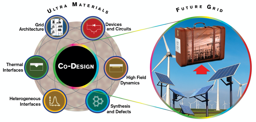
Ultra materials have applications in power electronics. The team strives to understand different aspects of their design, such as synthesis, thermal and electrical properties, and how they work in electronic devices so they can eventually be implemented in the energy grid. Graphic courtesy of Michael Northrop/Knowledge Enterprise Research Development/ASU
Using fewer components also helps reduce the complexity and size of the power electronics.
“There’s already been a lot of work over the years on materials that have wider band gaps than silicon, such as silicon carbide and gallium nitride,” Goodnick said. “Ultra materials are a step beyond that. They have almost twice the band gap of those materials and would be even better for these power electronics applications.”
Ultra materials could be used in the future to more efficiently convert energy from renewable sources and replace or augment electronic devices currently used in the power grid.
“You could have a smaller and more compact power conversion,” Goodnick said. “It would definitely reduce the footprint of power electronics, and it would potentially provide a higher switching voltage.”
By better understanding ultra materials and their applications, the research team can develop more efficient power conversion devices.
In-depth research creates and studies new ultra materials
Yuji Zhao, associate professor of electrical engineering, is involved in three of the project’s four thrusts: material synthesis, characterization and testing.
“At my lab, we have a metalorganic chemical vapor deposition (MOCVD) system, which is a $2 million investment from the Fulton Schools, and we use it to synthesize the new materials that will be the basis for our research,” Zhao said. “I will also be involved in the characterization of the material, looking at material properties, such as how defects interplay with electronic properties. I will also be involved with fabricating devices that can test the electrical and thermal properties of the material.”
Zhao and the rest of the research team will use the ASU NanoFab, a core facility for nanoscale fabrication and processing.
Marco Saraniti, vice dean of faculty administration and professor in the School of Electrical, Computer and Energy Engineering, is working with Goodnick on theoretical modeling of the materials.
“The software that I developed over the last 20 years allows me to input all the parameters of the [power electronics] device and simulate its operation,” Saraniti said. “Normally, this is only done electrically, but in my case I can simulate the electrical and thermal behavior of the device.”
Saraniti plans to simulate the generation of heat while the device is working and how heat is transferred from its inner parts to the outer parts and to the package in which the device is held.
Thermal management is important to study as it influences the longevity of a power electronics device. If the device gets too hot, it could cause catastrophic failures and can affect the performance of the whole system.
When ultra materials are used in voltage converters, thermal management is also important to consider as it can affect the efficiency of the device.
The EFRC project is likely to have a life well beyond DOE's four-year funding period.
“It is important for universities to have these kinds of long-term projects,” Saraniti said. “After this project is over, people will still keep working together to develop new ideas, and ASU has been very successful with these kinds of centers.”
More Science and technology

ASU joins Applied Materials' EPIC Center as inaugural university research partner
When the United States made the strategic decision in 2020 to reinvest in domestic semiconductor manufacturing, it confronted an…

ASU’s first human MRI enables breakthrough clinical studies
Arizona State University researchers now have access to the university’s first MRI system approved for human scanning, opening…

Being kind to oneself protects parents from depression
Burning dinner. Shrinking your child’s favorite T-shirt in the laundry. Losing your temper and snapping at your child.The…