ASU, Deca Technologies partner on advanced packaging research and development
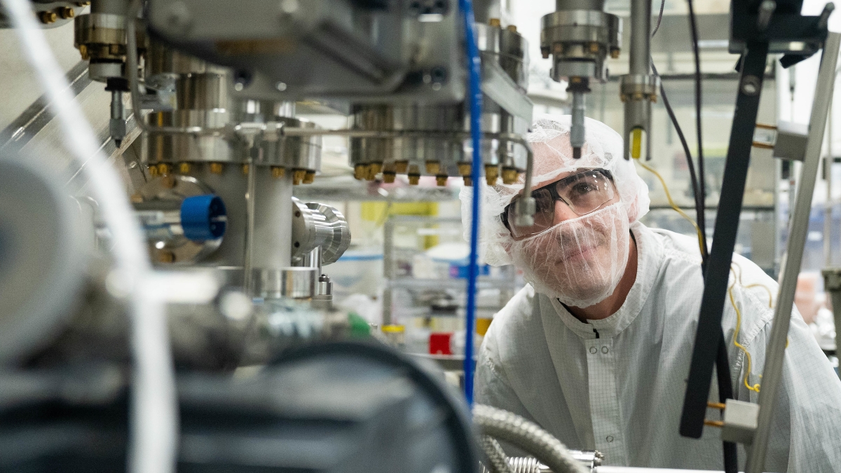
Researcher Tray Moraca inspects a piece of equipment at the MacroTechnology Works research facility. Photo by Samantha Chow/Arizona State University
While there is some difference of opinion about its obsolescence, there is little debate that Moore’s Law is slowing down.
Named after the co-founder of Intel, Gordon Moore, in 1965, Moore’s Law reliably predicted the pace of computing progress by introducing the tenant that “the number of transistors on a microchip doubles every two years.”
The formula of more transistors on smaller microchips has meant a steady march toward miniaturization, more power and lower costs.
But as computing speeds get faster and devices continue to get smaller, Moore’s Law is under duress; and as AI and big data become more prevalent, the stress on computing systems is magnified.
As America seeks to re-emerge as a world leader in semiconductor manufacturing, research and development, catching the next wave of innovation is important. Most experts agree that it will be in the area of advanced packaging.
That’s what makes Arizona State University’s new partnership with Deca Technologies, a premier provider of advanced wafer- and panel-level packaging technology, so important.
Announced this week, ASU and Deca will be collaborating to create North America’s first Fan-Out Wafer-Level Packaging (FOWLP) research and development capability.
The new Center for Advanced Wafer-Level Packaging Applications and Development is set to catalyze innovation in the U.S., expanding domestic semiconductor manufacturing capabilities and driving advancements in cutting-edge fields such as artificial intelligence, machine learning, automotive electronics and high-performance computing.
The center will combine state-of-the-art advanced packaging technology, equipment, processes, materials, expertise and training, fostering the development of new capabilities from proof of concept to pilot scale.
ASU is the first university implementation of Deca’s M-Series fan-out and Adaptive Patterning technologies, with the support of the Department of Defense’s Microelectronics Commons.
Learn more about the SWAP Hub
• New chief operations officer to help ramp up SWAP Hub advancements
The center will include integration with the university’s MacroTechnology Works center at ASU Research Park in Tempe, and will be an enhanced capability that will advance projects within the ASU-led Southwest Advanced Prototyping (SWAP) Hub.
The SWAP Hub is part of the Microelectronics Commons, a network of regional technology hubs coordinated to deliver on projects requested by the Department of Defense as part of the CHIPS and Science Act — the federal legislation that aims to expand America’s global leadership in microelectronics. As part of the CHIPS Act, Congress recognized the importance of packaging and appropriated $3 billion to establish a new National Advanced Packaging Manufacturing Program.
“This is at the heart of the next generation of innovation in microelectronics and everything it enables,” said Zak Holman, vice dean for research and innovation in ASU’s Ira A. Fulton Schools of Engineering. “Deca has developed a unique technology and ASU brings extraordinary capacity that will provide the resources to leverage Deca’s technology in ways that will be a differentiator for the work we are doing together through the SWAP Hub.”
The partnership will help make ASU a university leader in advanced packaging — a “back-end” part of the semiconductor manufacturing process that uses sophisticated technology and aggregates components from various wafers. Introduced more than 20 years ago, advanced packaging is now gaining significant momentum as the next pathway for breakthroughs in semiconductor technology.
“ASU is thrilled with the partnership with Deca, a company that is at the forefront of transforming the way the world builds advanced electronic devices,” said Sally Morton, executive vice president of ASU’s Knowledge Enterprise. “This partnership builds on the great work ASU is doing as one of the nation’s most productive research institutions, generating new ideas, technology and business with cutting-edge companies like Deca Technologies and others to positively impact our students, faculty and the communities we serve.”
The initiative offers both research and workforce development opportunities for ASU faculty and students engaging in the work of the new center, providing training for the high number of technicians who are needed domestically — including in greater Phoenix, home to Intel, TSMC, AMKOR and others.
In collaboration with Deca, ASU is committed to establishing onshore access to these advanced packaging capabilities. This entails acquiring, installing and implementing a comprehensive set of process and metrology equipment at the facility, capable of accommodating both 200mm and 300mm device wafer formats, as well as 300mm M-Series molded fan-out wafers, providing unparalleled flexibility for a diverse range of customers and applications.
“With the industry’s leading fan-out technology as a foundation, we’re excited about the possibilities this new center brings to Arizona as well as the broader U.S. semiconductor industry,” said Tim Olson, Deca’s founder and CEO. “Through ASU and Deca’s collaboration, unprecedented access for industry, academia, government and others opens the door to accelerate innovation and bolster U.S. technology leadership.”
ASU and Deca will apply these new capabilities to advance DoD Microelectronics Commons projects through the SWAP Hub and other R&D activities. The SWAP Hub submitted its first tranche of project proposals to DoD in February with decisions on additional funding expected later this year.
More Science and technology

The science behind chronic stress
Stress comes in many shapes and sizes. There’s the everyday stress of preparing for a final exam or being stuck in traffic. And the more significant stress of losing a friend, family member,…

ASU planetary scientist to be inducted into the National Academy of Sciences
The National Academy of Sciences is inducting School of Earth and Space Exploration Director Meenakshi Wadhwa into the 2023 class of new members for her pioneering work in planetary sciences and…
Unlocking the potential of AI for homeland security
“Can we do what we're doing now cheaper, more efficiently, more effectively?” Adam Cox, director in the Office of Strategy and Policy at the Department of Homeland Security Science and Technology…