ASU announces seed funding project partners for SWAP Hub
Will set the stage for expanded defense microelectronics prototyping projects
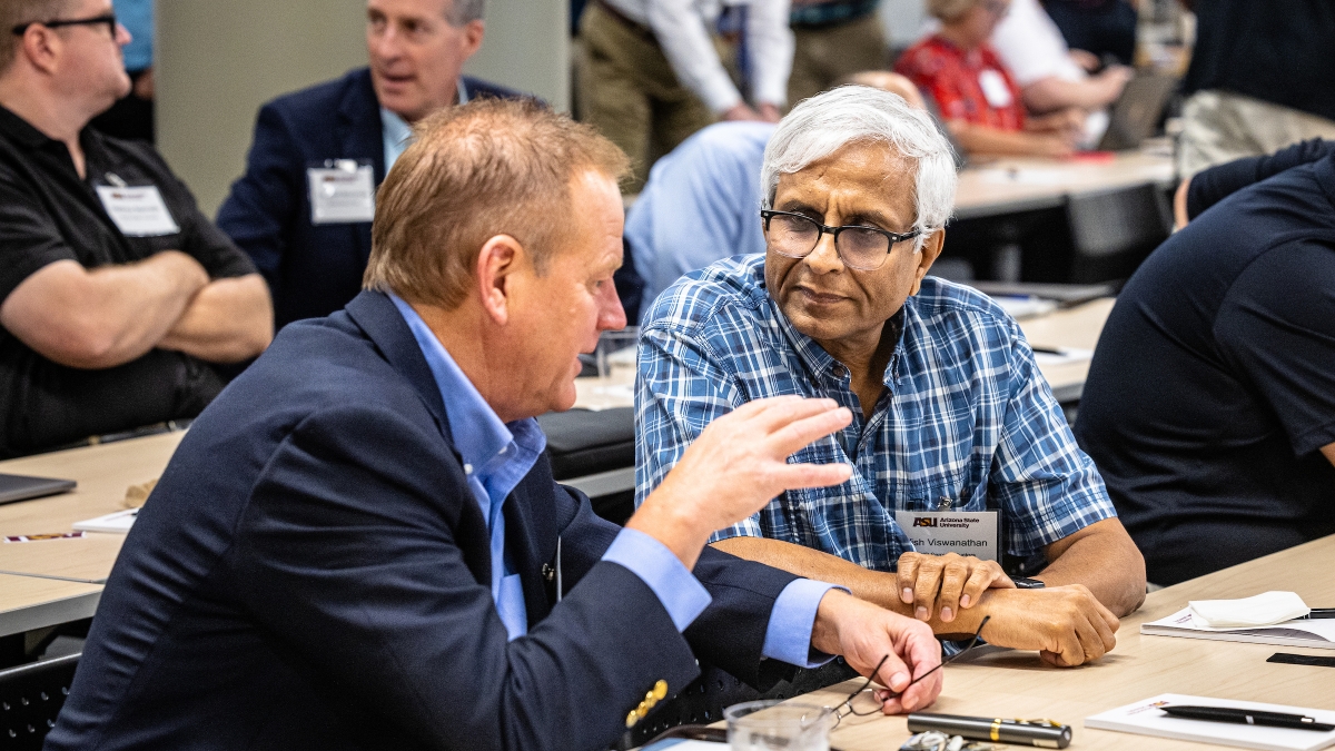
Tim Olson (left), founder and CEO of DECA in Tempe, chats with Vish Viswanathan of NXP Semiconductors during a Southwest Advanced Prototyping Hub workshop in July. Photo by Charlie Leight/ASU News
In advancing a vision for building a microelectronics ecosystem that can serve both the state of Arizona and America’s national agenda for semiconductor research, development and manufacturing, time is a factor, speed matters and so does collaboration.
Arizona State University is pushing ahead to do all that it can to have partners in place and be prepared when investment dollars begin to come from the federal government’s CHIPS and Science Act by advancing on the work that needs to be done with industry and to build a stable workforce.
One important piece of that work is to begin activating the Southwest Advanced Prototyping Hub, or SWAP Hub. The SWAP Hub is a proposed microelectronics innovation and prototyping hub submitted to the National Security Technology Accelerator for consideration as part of the Microelectronics Commons, a $1.63 billion Department of Defense program funded by the 2022 CHIPS and Science Act.
This week, ASU announced teams selected for four seed funding projects that will begin the activation of the hub, including Sandia National Laboratories, Siemens, NXP, Synopsys, NI, Northrop Grumman Mission Systems, Lockheed Martin and Intel.
To be eligible to apply for seed funding, applicants were required to have at least one ASU principal investigator and at least one SWAP Hub industry partner of the proposed SWAP Hub.
Projects were selected based on criteria that complement ASU’s goals of getting to work now and setting the stage for expanded defense microelectronics prototyping projects.
The seed project recipients had to demonstrate:
• Alignment with DoD microelectronics needs.
• Likelihood of seeding a large, impactful SWAP Hub project.
• Project approach, plan and feasibility.
• Team eligibility and project partner commitment.
The four chosen projects will explore immersion cooling for three-dimensional integrated circuits, develop reliable and reconfigurable gallium nitride-based radio frequency power amplifiers for advanced communications, establish built-in monitoring of artificial intelligence hardware running on edge devices, and evaluate the scaling of high-frequency and high-power diamond semiconductor devices.
“These seed projects bring together researchers from ASU, Sandia, microelectronics companies and defense primes — teams that have all of the players needed to transfer university and national lab technologies into defense products, which is a primary goal of the Microelectronics Commons,” said Zachary Holman, vice dean for research and innovation in ASU’s Ira A. Fulton Schools of Engineering. “The projects jumpstart the microelectronics collaborations that our nation needs.”
RELATED: Workshop brings academic, industry partners together to collaborate on CHIPS Act projects
More details on the project criteria:
• Alignment with DoD microelectronics needs: The proposed project aligns with one or more of the topics identified in the 5G/6G, AI Hardware or Commercial Leap Ahead Technologies subsections of National Security Technology Accelerator's "Attachment C: Technical Guidance" document.
• Likelihood of seeding a large, impactful SWAP Hub project: If the seed project is successful, it will lay the foundation for a competitive proposal to the National Security Technology Accelerator for a much larger, defense-focused microelectronics prototyping project (e.g., $5–30 million in scale, with a starting technology readiness level of 3–4) to be executed within the SWAP Hub and transitioned to industry. That is, the seed project will demonstrate key technology innovations or retire early risks that are barriers to successful prototyping, and, in so doing, display the team’s capability for effective collaboration.
• Approach, plan and feasibility: The project’s approach to solving the problem or answering the question is innovative, differentiated from the existing state of the art and technically sound. The plan to execute the project is clear and well developed, with SMART (specific, measurable, achievable, relevant and timely) milestones to monitor project progress. The scope of the project is consistent with a six-month timeline and an investment of $50,000 per institution.
• Team eligibility and project partner commitment: The team unites members of the SWAP Hub, is qualified to conduct the proposed research, is eligible for future Department of Defense project funding, and has the capability and resources to complete the project plan. All team members are fully committed to the success of the project, as evidenced through the partners’ letters of commitment.
More Science and technology

ASU researchers develop special microphone to verify human speech
Deepfakes have become a large societal concern with the advent of video and audio content generated by artificial intelligence, or AI. A deepfake is a convincing imitation that blurs the lines…

Leading students toward a future of renewable energy
Nicholas Rolston, assistant professor in the School of Electrical, Computer and Energy Engineering, one of the Ira A. Fulton Schools of Engineering at Arizona State University, has found his passion…
SPARCS mission spacecraft bus delivered to ASU for final assembly
The Arizona State University team that is building the NASA-funded Star-Planet Activity Research CubeSat, or SPARCS, cleared a major milestone this week — receiving its spacecraft bus at the School…