A new process being developed by Arizona State University researchers enables color printing on a microscale with a simple, inexpensive additive manufacturing process.
Chao Wang, an assistant professor of electrical engineering in the Ira A. Fulton Schools of Engineering at ASU, has invented a solution-based additive manufacturing process to “paint with light” on glass and plastics. Wang’s novel printing method uses light to control the photochemical reduction of metal microstructures on an engineered optical material.
The technique opens new avenues for color printing on the microscale, including printing on surfaces such as wearable optical devices and flexible displays. It also allows for the creation of colored, high-resolution pictures without applying complex and expensive semiconductor-processing techniques.
A peer-reviewed manuscript on this work, “Structural color printing via polymer-assisted photochemical deposition,” authored by Wang, Yu Yao, a Fulton Schools associate professor of electrical engineering, and students working in their labs, was recently published in the research journal Light: Science & Applications.
Wang’s new technology is based on polymer-assisted photochemical metal deposition, or PPD. The new technology is used at room temperature, is nontoxic and provides a solution-based additive manufacturing process that does not require any heating, vacuum deposition or etching steps. This allows for the printing of ultrathin and smooth silver surfaces to act as the top light-absorptive film in the engineered optical material, which also includes thick and reflective films on the backside.
Wang says this advance sprang from the team’s previous work in creating a new additive manufacturing technique for high-quality 3D printing of metal objects.
“This is an extension of that work,” Wang says. “Unlike conventional metal printing techniques that rely on high-temperature laser heating, our developed technology is a solution-based printing process. Here, we show it is also applicable in creating more complex photonic structures.”
The team introduced a polymer in the precursor solution that functions like “sticky hands” to connect the reduced metal nanoparticles together into continuous and smooth films. This means the printed metal film is a composite of metal nanoparticles and a small amount of the sticky-handed polymer.
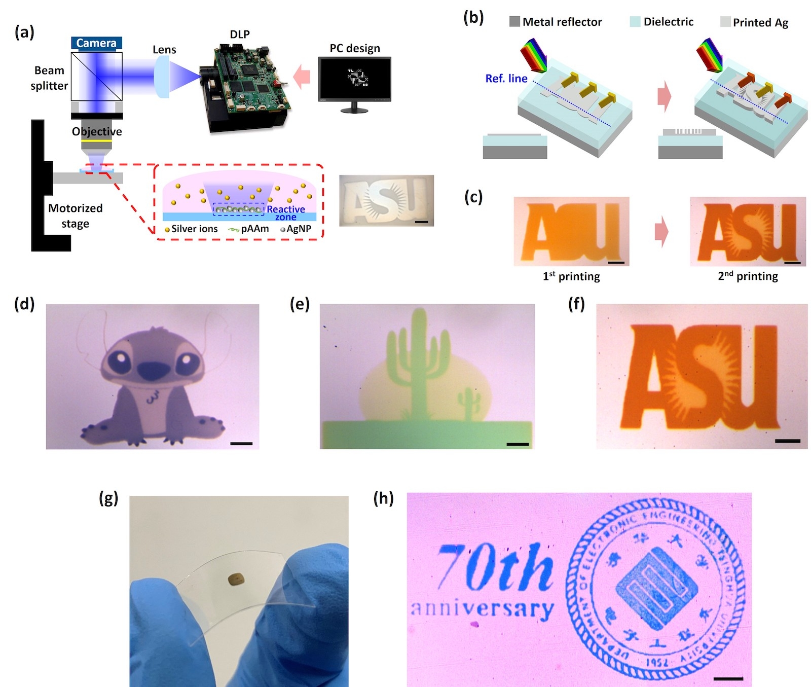
ASU researchers were able to print blue, green, yellow and orange color pictures with high contrast using Chao Wang’s new polymer-assisted photochemical metal deposition process. To demonstrate its versatility in printing, the paper’s first author, Shinhyuk Choi, an electrical engineering graduate student in Wang’s lab, printed pictures of a character named Stitch in blue and purple (d), an image of a cactus in green and yellow (e), and versions of ASU’s logo in orange and yellow (c and f). Figure (a) shows a schematic illustration of the polymer-assisted photochemical deposition, or PPD, printing setup and an example of a printed ASU logo (scale bar: 500 μm, or about 0.0197 inch). In figure (b), a 3D scheme shows the printing of a multilayered film stack into microstructures. Figures (d-h) are demonstrations of the feasibility of printing complex structures with various colors. The photo in figure (g) shows a fabricated Fabry-Perot Cavity on a polyethylene terephthalate, or PET, plastic substrate with gentle bending. Figure (h) depicts optical images of a produced colored logo of the Department of Electronic Engineering – Tsingha University, Wang’s alma mater, on a dielectric-coated metallic layer with a scale bar representing 100 μm (about 0.0039 inch). Images courtesy of Chao Wang
To vividly display color in the printings, the authors engineered optical material in the form of a multilayered, thin-film structure called a Fabry-Perot Cavity. It functions similarly to the colorful pigments from paintings that absorb light from specific wavelengths. The Fabry-Perot Cavity absorption is affected both by the thicknesses of printed metal films — controllable even when thinner than 10 nanometers — and the designed film stack dimensions the films are printed on.
“Photons interact with the cavity structures to absorb a particular wavelength of light allowing you to display a new color,” Wang says.
In this process, ultraviolet light is used to program a photochemical reduction of silver in a solution at room temperature. Therefore, light is used directly to “print” color pixels down to micrometer sizes.
“It has been a very fun experience to be able to use light to create microstructures that can, in turn, control light,” Wang says. “This is a good example of how multidisciplinary thinking helps in research.”
Top image courtesy of Unsplash
More Science and technology

The science behind chronic stress
Stress comes in many shapes and sizes. There’s the everyday stress of preparing for a final exam or being stuck in traffic. And the more significant stress of losing a friend, family member,…

ASU planetary scientist to be inducted into the National Academy of Sciences
The National Academy of Sciences is inducting School of Earth and Space Exploration Director Meenakshi Wadhwa into the 2023 class of new members for her pioneering work in planetary sciences and…

Unlocking the potential of AI for homeland security
“Can we do what we're doing now cheaper, more efficiently, more effectively?” Adam Cox, director in the Office of Strategy and Policy at the Department of Homeland Security Science and Technology…